This article discusses in detail the anti-interference topic of DC-DC converters. Let's talk about DC-DC converters. Since the birth of electronics, there has been an old saying... "All problems are DC issues."
Of course, DC refers to "direct current", that is, a unidirectional current passing through a conductor from point A to point B in a circuit. We know that the "problem" mentioned here is very simple, that is... the problem. So why are all issues DC issues?
We know that current and electrons are simply the energy produced by currents in various conductors and devices in a complete circuit system. Therefore, in the final analysis, it is an energy conversion. Energy is the ability to do work in two forms: 1) potential energy and 2) kinetic energy. Potential energy is an inactive energy storage (such as the voltage between battery terminals). Kinetic energy is the energy generated when potential energy is converted into an active state (such as current flowing through a bulb). Electronics is simply the science of transforming potential energy (voltage) into kinetic energy (current) by controlling the current in various conductors! Ohmic 'DC Law' must always satisfy the energy conversion to make a difference! Therefore, each part of the circuit input and output, whether or not with AC function, must be well designed for the DC structure of the circuit to effectively support any form of energy conversion. In other words, if the circuit DC design is poor, it is impossible to achieve AC performance.
This situation puts great pressure on the designer, and needs to master the high-level expertise in multidisciplinary fields based on the “simulation design†between the power supply and the ground. In order to convert direct current (DC) with low noise under various voltage conditions with respect to various input signals, it is first necessary to select the correct DC-DC converter. DC-DC converters come in a variety of sizes and types: converters include linear, switch mode, and magnetoelectric. Moreover, the boost (step-up) and buck (step-down) functions use a variety of energy conversion circuits. Knowing these circuit types correctly can avoid performance degradation when used. Later, we can analyze the devices introduced by industry leaders, such as the National Semiconductor's recently launched Simple Switcher power module.
"All problems are DC problems..." Knowing this when considering DC-DC converters can lay the foundation for good circuit design.
Linear regulator
Linear regulators are the most basic components of all DC-DC converters. The linear regulator is a voltage regulator that operates in a "linear region" relative to a switching regulator operating in the "non-linear" switching mode region (which we will discuss later). The linear regulator must meet the rated power supply for the load (low noise to an acceptable level) while reducing the output impedance requirements so that the voltage gain is not affected by the load impedance value. The linear regulator acts as a variable resistor that regulates the voltage divider network to maintain a constant output voltage while providing various load currents.
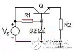
figure 1
Figure 1 shows the schematic of the linear regulator. The figure shows a "series" linear regulator circuit because the regulation device (transistor Q) is in series with the load R2. The circuit regulates the Zener diode DZ output voltage (because the transistor base current is a small fraction of the Zener to R1 bias current). The transistor emitter output voltage is one diode drop below the Zener voltage and has sufficient current gain to drive the high output value Iout (via R2). Although the circuit has good output voltage regulation (as long as Q is operating in the linear region), it still senses load, power supply variable (Vs), noise, and power supply ripple. Some of these problems can be solved with a negative feedback circuit sensing circuit output. At other times, this circuit is often used as a voltage reference to support more advanced linear regulator designs. When designing or selecting a linear regulator, you must also carefully consider the electrical noise, the ripple generated by the power supply Vs to Vout, and the common-mode voltage that may be coupled in the regulator output.
For example, when selecting a linear regulator, the circuit power requirements and regulator output characteristics must be carefully determined. Take National Semiconductor's LM340/LM78XX series of three-terminal positive voltage regulators as an example. These linear regulators are standard devices with basic design elements in the industry. In general, some devices specify a fixed output voltage (typically Vs-Vout 2V) at a fixed input voltage and a maximum fixed output load current Iout.
Load regulation defines the change in output voltage (Vout) over a given output current range (Iout). Since the output voltage is close to the Vs input voltage, the series output voltage regulation transistor (Q1) near saturation state and voltage/current gain attenuation will cause the load regulation characteristics to deteriorate. This also applies to line regulation. Line regulation changes the output voltage (Vout) over a given input voltage (Vs). Similarly, the Vo line regulation generally defines a low level Vs in the mV level. As the input voltage changes, the mV stage can be amplified ten times (compared to the output voltage), and the gain is obtained when the output voltage regulating transistor approaches the breakdown point. It will fall. Line regulation also implements ripple rejection (Vin/?Vout ratio) and should be greater than 60 dB to prevent AC ripple from entering the linear regulator DC input voltage through the input supply line. Ripple suppression is critical for analog systems that require accurate gain and dc accuracy. Power ripple into the linear regulator can also be improved by adding the necessary power supply decoupling capacitors to further filter out unwanted ripple in the linear regulator input and output (we will discuss power supply decoupling issues later). ).
Decoupling diagram (Vout is grounded by L in series with two capacitors)
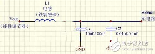
figure 2
Some important design concepts for proper decoupling to reduce noise are shown in Figure 2. Place a large electrolytic capacitor C1 (typically 10 μF – 100 μF) near the output of the linear regulator (within 2 inches). This capacitor acts as a charge bank that instantly supplies current to the load without having to supply charge through the regulator/inductor. The small capacitor C2 (typically 0.01 μF – 0.1 μF) should be placed as close as possible to the load. The purpose of this capacitor is to reduce the high frequency noise of the load. All decoupling capacitors should be connected to a large area of ​​low impedance ground plane to reduce impedance. The linear regulator output inductor L1 (usually a small ferrite bead) limits the noise inside the system and suppresses high frequency noise from external loads while avoiding internal noise (from the load) propagating to other parts of the system.
EO2 is an Ethernet extender over UTP cable. One EO2 at the network end can support one or multi remote models and their connected IP network devices. This EO2 can transmit over telephone line, Ethernet cable, and twisted pair. It is provided with excellent lightning protection and anti-interference capacity. In the real work environment, the network bandwidth could reach up to 60Mbps. With the Ethernet extended to 750meter, it has enlarged the Ethernet network application area, cutting down the project cost by using Cat5e or Cat6 cable.
N-net EO2 series have POE function, powering remote EO2 transceivers and their connected IP network device, default as a master terminal.
Ethernet And Power Over UTP Cable Converter
Ethernet And Power Over UTP Cable Converter,Power Over Ethernet,UTP Cable Converter,POE over UTP Cable Extender
Shenzhen N-net High-Tech Co.,Ltd , http://www.nnetswitch.com