1 Introduction
With the increasing demand for radar applications and the rapid development of digital signal processing technology, the design of radar receiving systems is increasingly expected to conform to the design philosophy of software radio, that is, the ADC is as close as possible to the antenna, and the received analog signal is digitized as early as possible.
The digitized IF signal is usually based on FPGA to achieve digital down conversion to obtain baseband I/Q signal. However, as the carrier frequency and bandwidth of the signal continue to increase, a higher speed ADC is required to complete signal sampling, so the processing requirements for digital down conversion are also higher. The higher it is. In the ultra-wideband radar receiving system, the high-speed data rate makes the FPGA-based wideband digital down-conversion algorithm no longer suitable for traditional serial structure implementation. This paper introduces an ultra-wideband digital down-conversion based on parallel multi-phase filtering structure. The design method, its parallel pipeline processing method makes high-speed data without buffering, and the processing bandwidth is also greatly improved.
2. Design principle
According to the band-pass sampling theorem, the sampling rate sf and the signal intermediate frequency cf are in the digital intermediate frequency receiving system. When the content is satisfied (where M is a positive integer), the digital mixing algorithm is the simplest, especially in the ultra-wideband digital receiving system with high sampling rate. Satisfying this condition can simplify the design and facilitate engineering implementation.
In the ultra-wideband digital receiving system of this paper, both the sampling rate and the receiving bandwidth are large, and the low-pass filter design adopts a multi-phase structure. Let the impulse response of the low-pass filter be h(n) and its Z transform be:
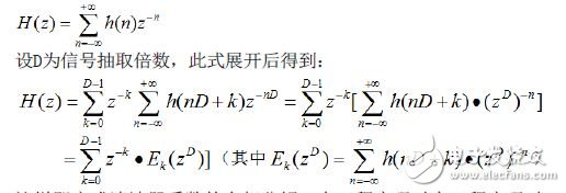
In this way, the multi-phase decomposition of the filter coefficients is completed. In the engineering implementation, the requirements of the hardware processing speed can be reduced and the real-time processing capability can be improved by adopting the method of first extracting and filtering as needed.
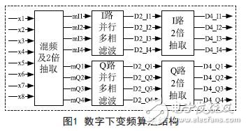
The digital down-conversion simulation and design is based on the FPGA system-level design tool System Generator (SysGen), which enables direct migration from the algorithm model to the FPGA hardware. The engineering implementation mainly includes three parts: digital mixing, parallel multi-phase filtering and data extraction. The digital mixing process realizes double extraction at the same time. The parallel multi-phase filtering obtains the baseband I/Q data of the large bandwidth signal, and then the baseband. The extraction of the smaller bandwidth can be achieved by performing a 2x or multiple extraction of the signal. Taking the parallel eight-phase filter decomposition structure as an example, the structure of the digital down-conversion algorithm is shown in Figure 1.
3. Algorithm implementation
In the ultra-wideband digital receiving system of this paper, the signal intermediate frequency is required to be 400MHz, the sampling rate is 1600MHz, and the input signal bandwidth includes 600MHz and 350MHz. According to the requirements of the subsequent processing system, the digital baseband signals are respectively extracted by 2 times and 4 times, and the extracted data rates are 800 MHz and 400 MHz, respectively.
High-speed ADC selects TI's ADC083000, its sampling rate and full power bandwidth are up to 3GHz; FPGA selects Xilinx Virtex-6 series XC6VSX315T, which has more DSP48E resources, which is very suitable for digital down conversion algorithm. Multiple digital filter designs.
3.1 High speed digital signal preprocessing
The high-speed digital IF signal after ADC sampling is input to the FPGA through a parallel bus with a speed of 400MHz. Such a high-speed signal is obviously not easy to directly perform digital down-conversion processing in the FPGA. In order to adapt to the processing speed of the FPGA for digital down conversion, to ensure that it works stably at normal temperature and high temperature, it is first necessary to reduce the speed of the high speed digital signal. Virtex-6 series FPGAs have a dedicated double data rate register IDDR to double the data rate, and the falling edge data is controlled by the inversion of the input clock. The algorithm is implemented as shown in Figure 2.
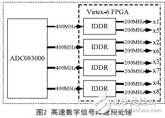
After the speed reduction process, the four parallel high-speed signals input to the FPGA and the 400MHz high-speed signal become eight parallel, low-speed signals with a rate of 200MHz. This data rate is very suitable for FPGA processing.
3.2 Digital Mixing
Since the signal intermediate frequency 400MHz and the sampling rate 1600MHz are in accordance with fc/fs=1/4, the digital local oscillator has only a simple sequence of 1, -1 and 0, and the digital mixing process becomes an addition and subtraction operation. Assume that the 8 parallel signals after the speed reduction preprocessing are (x1, x2, x3, x4, x5, x6, x7, x8), then the parallel I channel parallel signals are (x1, 0, -x3, 0, x5). , 0, -x7, 0), Q parallel signal is (0, x2, 0, -x4, 0, x6, 0, -x8,).
In this paper, the maximum bandwidth of the input signal is 600MHz, so the minimum number of extraction after digital down conversion should be 2, and after digital mixing, I/Q each generates 4 channels and behaves as 0 data, so that the mixing process can be doubled. After decimation, the four parallel tributary signals of the I path are (x1, -x3, x5, -x7), and the four parallel tributary signals of the Q path are (x2, -x4, x6, -x8). In actual engineering implementation, the digital mixing process only needs to divide the input 8 parallel AD signals into two groups, and the addition and subtraction operations are processed together with the parallel parallel multiphase filtering.
3.3 Parallel polyphase filtering
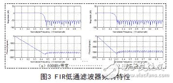
The input signal contains two bandwidths of 600MHz and 350MHz. In order to meet the needs of multi-phase decomposition and reloading of filter coefficients, the FIR low-pass filter is designed to be 63-order and 64-factor. The frequency response characteristics are shown in Figure 3.
The most important part of the parallel polyphase filtering algorithm is the coefficient decomposition. The coefficient decomposition first performs two-phase decomposition, and then each performs four-phase decomposition, and obtains the coefficients of the eight branch I/Q signals.
After digital mixing and 2x extraction, the I signal retains only the odd branch, the Q signal retains only the even branch, and the filtering algorithm is actually a multiply-accumulated linear convolution process, so I low pass filtering The even-numbered portion of the FIR filter coefficients is used, and the Q-channel low-pass filtering uses only the odd-numbered portions of the FIR filter coefficients, so the filter coefficients can be first decomposed into two phases. In order to meet the coefficient reloading design requirements, the coefficient length of each branch should be the same after parallel polyphase decomposition, so the number of FIR low-pass filter coefficients should be even N. Assume that the filter coefficient is 1 2 3 ( , , , ..., ) N hhhh , the coefficients of I and Q after two-phase decomposition are 2 4 ( , ,..., ) N hhh and 1 3 1 ( , ,..., ) N hhh .
FTTH Fiber Optic Socket Terminal Box, fiber termination box provides a mini density wall-mounted solution for next generation networks, which aims to provide and manage minimum numbers of fibers in a limited space.
It is normally installed in the way of wall-mounted. Widely used in FTTH access network, telecommunication networks, CATV networks, data communications network, local area networks, indoor and outdoor application.
Mini FTTH terminal box is designed specially for FTTx application, which suits for jointing fibers pigtail and it protects fiber optic splices and helps to share out the connectivity to individual customers. Optical Termination Box is designed to connect raiser/distribution cables to subscriber`s drop cable in FTTx networks. It has 1 input port and 1 output ports on the bottom and it is easy to install on the wall.


FTTH Fiber Optic Socket Terminal Box
Optical Fiber Terminal Box,Fiber Access Termination Box,Fiber Optic Terminal Box,Fiber Optic Junction Box,Fiber Optic Cable Junction Box
Sijee Optical Communication Technology Co.,Ltd , https://www.sijee-optical.com