Summary
This article refers to the address: http://
Powering RF power amplifiers in handheld devices has always been a difficult design because on the one hand, it is necessary to improve the working efficiency of RF power amplifiers to extend the working time of the battery, and on the other hand, it can not reduce the work of the power amplifier while improving work efficiency. Performance, so it must be provided with a high efficiency DC power supply that meets the requirements. The conventional way is to connect the power supply terminal of the power amplifier directly to the battery, but this mode of operation will make the power amplifier work very low and cannot meet the requirements of high efficiency and low power consumption. Texas Instruments' SuPA (Supply for Power Amplifier) ​​series of DC-DC products have been innovative in their working mechanisms, using Average Power Track technology and Envelop Tracking to optimize RF power amplifier operation. Time power consumption, which improves the working efficiency of the power amplifier and prolongs the working time of the battery. This article focuses on the working principle of the average power tracking technology and the application design of SuPA, so that design engineers can quickly understand and apply this technology to achieve efficient power amplifier power supply design.
1 Introduction
At present, more and more handheld devices are required to meet the longest working time. The common methods are: on the one hand, optimizing the system software, turning off unused software to save more power, and prolonging the working time of the battery. This is very efficient in optimizing the power consumption of the application processor; on the other hand, optimizing the hardware design of the system, using a low-power, high-efficiency power management unit, is very effective in optimizing the power consumption of the RF unit and the application processor unit. SuPA is a power supply for driving power amplifiers in RF units. In addition to the high working efficiency of DC-DC, it also adopts average power tracking technology (APT) to match different power-to-voltage voltages when working with RF power amplifiers. Demand, dynamically adjust the output voltage to power the amplifier to meet efficient work efficiency.
2. What is Envelop Tracking?
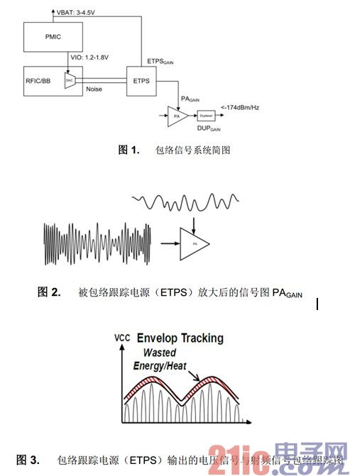
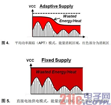
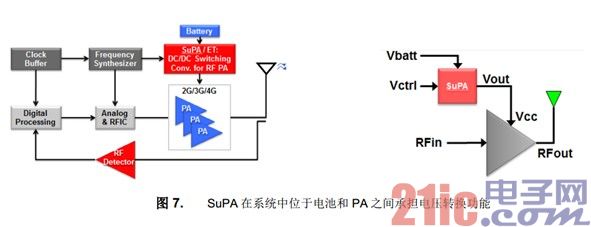
In short, it is the technology that establishes the connection between the working voltage of the power amplifier and the input RF signal so that they can follow each other in real time, thereby improving the working efficiency of the power amplifier. According to theoretical calculations, it is relatively straightforward to use the battery power supply mode, which can help The system saves 65% of power consumption and will be supported by SuPA's next-generation products. Its basic principle is: the RF processing unit and the baseband processing unit calculate the envelope signal according to the RF signal, the power level and the power characteristic parameter of the power amplifier (you can use the power amplifier's Look Up Table or the Shaping Table). (Envelop signal), while the differential DAC in the RF and baseband unit provides an analog reference signal. The ET power supply (ETPS) amplifies the envelope signal and sends it to the PA. At this time, the PA amplifies the RF signal, making the RF The signal and the operating voltage of the PA follow. Finally, the amplifier sends the amplified signal to the duplexer. The duplexer attenuates the signal outside the bandwidth and highlights the useful signal. Figure 1, Figure 2, and Figure 3 illustrate the signal conditioning process in this process.
3. What is the average power tracking technology (Average Power Track)
This method is also called Adaptive Supply. It is based on the pre-output power of the power amplifier and the power amplifier's own parameters (you can use the power amplifier's parameter lookup table Look-Up-Table) to automatically adjust the power amplifier's work. The voltage technique, according to theory, can help the system save 40% of its energy compared to the battery direct power mode. Compared to ET, APT is easier and more convenient to use and design.
SuPA's current products primarily support this model.
4. Development trend and characteristics of RF power amplifier
With the continuous increase of data services, it has been transferred from 2G to 3G and 4G, so the power amplifier is required to undertake more tasks. Therefore, it is required that the power amplifier has more working modes and frequency bandwidth to meet the requirements of different regions, and at the same time, it must meet higher requirements. The efficiency of the operation thus maintains the battery's long battery life. Therefore, in order to meet this requirement, the RF power supply using ET mode or APT mode is gradually becoming a trend. The following figure shows an example, its RF power supply unit can support 4 kinds of bandwidth. GSM/EDGE mode.

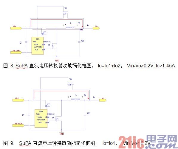
5. Position of SuPA in the RF unit
SuPA is the location of the power supply in the RF unit of the system. It is between the battery and the power amplifier. The battery voltage can be converted according to the power signal provided by the baseband unit and the RF unit and the signal of the power amplifier. The working voltage of the excellent working mode, the driving power amplifier works in the high efficiency mode, and achieves the purpose of saving electric energy.
6. SuPA working mechanism in APT mode
1. UCC27201 datasheet, Texas Instruments Inc., 2008
2. LM5035 datasheet, Texas Instruments Inc., 2013
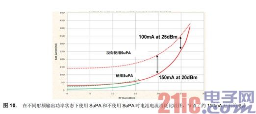
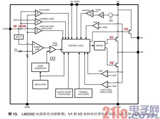
The internal topology of the SuPA power converter is the same as that of the conventional synchronous rectified step-down DC converter. There is no big difference, but its load dynamic response and active current assist bypass control (Active Current assist and Bypass) is It has been optimized so that it can respond quickly when load voltage and current change. The active current assist bypass function can quickly switch the converter to a similar load when the inlet voltage drops instantaneously or the load current increases instantaneously. Switch mode, there are two advantages to this: First, the battery energy can be quickly provided to the load to meet the load demand; second, small size, small current inductance can be used, when the load current exceeds the current limit of the inductor, then ACB The function switch V3 enters the working mode, and the additional load current is taken over to the load without the need for an inductor. Therefore, a small-sized inductor can be used to meet the ultra-compact design requirements, which is very important in practical application design. Its working process is: first, when the switch V2 is turned on, V1 is disconnected, and the inlet power supply will charge the inductor. At this time, the electromotive force at both ends of the inductor is "positive" on the left and "negative" on the right, when the inductor is charged. After completion, V2 will be disconnected and V1 will be turned on. At this time, the voltage across the inductor will be reversed, and the left side will be “negative†and the right side will be “positiveâ€, so the energy stored in the inductor will pass through the load, V1. Then return to the negative pole of the inductor, the inductor is more like a battery to power the load. The charging and discharging process of the inductor will be repeated, and the continuous current will be continuously supplied to the load. Its mathematical expression is: Vo=D*Vin, where D is the duty cycle, that is, the time when V2 is turned on. The proportion of the entire switching cycle. VCON is used to receive control signals from the RF processing chipset or baseband chipset. This signal is sent to the SuPA DC converter control unit to convert the output voltage and VCON voltage signal by A factor, so the output voltage and VCON. The signal will be converted according to the ratio of A times, namely: Vo=A*VCON; when the inlet voltage drops or the load current increases unexpectedly, the converter instantaneously over-current, so the active current-assisted bypass function (ACB) is turned on. Mode, V3 will adjust the voltage of the battery voltage or the inlet power supply before connecting to the system to meet the instantaneous large load current demand, but when the inlet voltage falls further to the output voltage or the pressure difference is within 200mV, V3 will be completely complete. Turn on, enter the true bypass mode, this is SuPA's unique control mode. For example, the 2G PA transient current tends to exceed 2A, so the bypass function will be very important; at 3G or 4G, the current demand Not too big, so SuPA works in a single DC-DC conversion mode to meet high efficiency requirements.
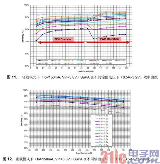
7 SuPA converter high efficiency working mechanism and efficiency curve
SuPA can work in both high-efficiency power-saving and low-noise modes. These two modes are automatically converted. When the load current is lower than 100mA, it works in the power saving mode (PFM/ECO, the switching frequency will be automatically reduced, and the switch will be reduced. Loss); when the load current exceeds 100mA, it works in low noise mode (PWM, constant switching frequency, meets large load current output), which ensures that SuPA can remain efficient under a wide range of load conditions. The working state achieves the purpose of saving power and prolongs the working time of the handheld device.
8 Internal circuit block diagram of SuPA in APT mode
Taking a detailed design description of the LM3242, the LM3242 is a 6MHz switching power supply for 3G and 4G power amplifiers. The output voltage is continuously adjustable from 0.4V to 3.6V with ACB mode (FB pin and VIN pin). The MOSFET between this function, multiplexed FB pin function), the maximum output current can support up to 750mA (DC-DC mode) and 1A (ACB mode), support automatic power saving and low noise mode; its next generation product The LM3243 can support up to 2.5A of output current with a separate ACB pin for active auxiliary current bypass mode, so the LM3243 can support up to 2G/3G/4G mode for richer functionality and wider application range.
It can be seen from its internal functional block diagram that the main switch tubes V1 and V2 are responsible for the step-down conversion function, which is in accordance with Vo=D*Vin, while the switch tube V3 is responsible for the ACB function, and the FB pins are multiplexed to take voltage feedback. And ACB energy output; VCON pin is used to receive the analog voltage signal from the RF unit or baseband unit. This signal is calculated by the processing chip of the baseband unit and the RF unit to calculate the RF signal information and the characteristic information of the RF amplifier. Converted into a variable voltage signal, this variable voltage signal is sent to the LM3242, so that the output voltage follows this variable input voltage signal, they can be described by mathematical formula: Vo = A * VCON, A = 2.5, VCON = 0.16V ~1.44V.
9 Schematic design and key power device design for SuPA in APT mode:
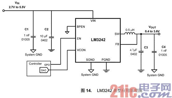
Figure 14 is a typical schematic diagram of the LM3242. In order to clearly illustrate the power device design process, the following two parts will be described.
Input and output capacitor design considerations:
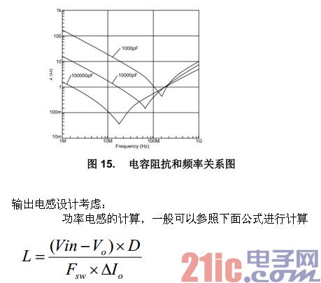
It can be seen from Figure 14 that the input capacitance is a combination of 1nF and 10uF. The reason for this is that the noise of different frequencies can be filtered out. The input noise can come from two parts: first, the noise from the input power bus. For example, the bus also supplies power to other loads, and the power of these loads is also from the DC-DC converter, so the power bus will superimpose very rich noise. Second, the self-switching noise from the LM3242, its switching noise is also the same. Will be superimposed on the input, so it may interfere with other load chips on the bus, so in actual design, the inlet will need more capacitors with different capacitances to meet the requirements of filtering different noise frequencies, such as 10pF or 100pF capacitors. It is also used that the optimum filtering frequency for capacitors with different capacitance values ​​is also different. For large-capacity capacitors, the frequency range that can be filtered out is relatively narrow, because its inflection frequency is relatively low. In the frequency of the inflection point, the impedance of the capacitor is in a downward trend, that is, the performance is a capacitive characteristic, but above the inflection point frequency, the resistance It is a rising characteristic, and it exhibits an inductive characteristic, so it no longer has a filtering effect, which is why it is necessary to match different capacitance capacitors, because the noise frequency is very rich, and a capacitance of capacitance is impossible to wideband. The noise is completely filtered out. In addition, it should be noted that the capacitance of the small capacitance of the same capacitance value and the same withstand voltage shows a wider capacitive bandwidth, which is mainly a small-sized capacitor, and its internal parasitic inductance is smaller. At the same time, its effective capacity is lower, so the characteristic is that the bandwidth of filtering noise is wider. From the figure, it can be seen that the capacitor of 01005 package with small capacity but smaller size can filter out the noise band. width.
As can be seen from the formula, the smaller the ripple current, the larger the inductance, and the smaller the ripple current, the smaller the ripple voltage generated on the output capacitor (ripple voltage = ESR* of the output capacitor) Ripple current), but the size of the inductor will become larger, which is not conducive to small size design. Therefore, in actual design, it is necessary to balance the relationship between inductance, ripple current, and inductor size. When selecting the inductor, in addition to satisfying the inductance parameter, consider the maximum current that the inductor can withstand, that is, the IRMS current value, and also consider the saturation current value of the inductor, that is, ISAT, if the total current flowing through the inductor is ITOTAL =IDC+IRIPPLE Exceeds ISAT, which will make the inductor saturated and lose the inductance characteristics, that is, the inductor becomes a wire, which causes the converter to fail and is damaged. Generally, the engineering quick evaluation can take 1.5 times Io. As a suitable selection criterion, such as the output load current is 1A, it is better to select the effective current IRMS of the inductor is 1.5A; also note that the inductor with shielding function should be selected as much as possible to reduce the DC-DC conversion. The interference caused by the external environment when the device is working.
10 SuPA PCB design and PCB board stack design
1. Position of the power device (input, output capacitor and inductor)
As shown below,
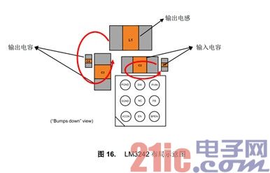
It can be seen from the figure that the inlet capacitors C1 and C2 are placed closest to the PVIN pin of the chip, and the output capacitor is placed closest to the output of the inductor. The reason for this is to keep the power loop of the input terminal. (Chip, C1 The loop of the circuit composed of C2 and ground) and the output power loop area (output inductor, C3, C4, ground) are the smallest, which can effectively reduce the interference of the switching power supply noise to the external environment. This is in the design of the RF circuit. Points to think carefully.
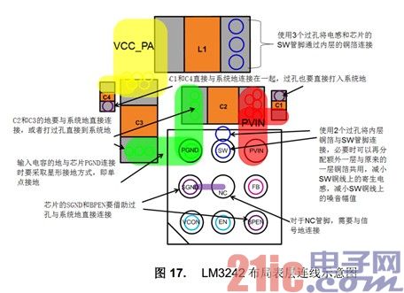
2. Power device and chip connection and PCB board stack definition
PCB board stack design example:
Surface layer: Used to connect wires that flow large currents, such as input, output capacitors, and inductors.
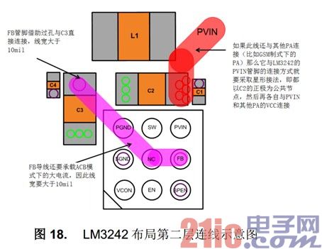
The second layer: the connection signal can be placed in this layer, note that the FB pin is multiplexed (used as ACB) will carry a relatively large
Current, so you need to use a line width connection of more than 10 mils.
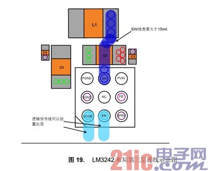
The third layer: the connection to the SW can be placed in this layer, the SW is used to carry the peak current greater than 1A, so the line width needs to be greater than 15mil,
In some applications, it is even necessary to assign two layers of SW copper wire (two layers of superposition) at the same time to reduce the parasitic inductance and reduce the copper wire as much as possible.
Dv/dt, which is the switching noise ringing amplitude on the SW.
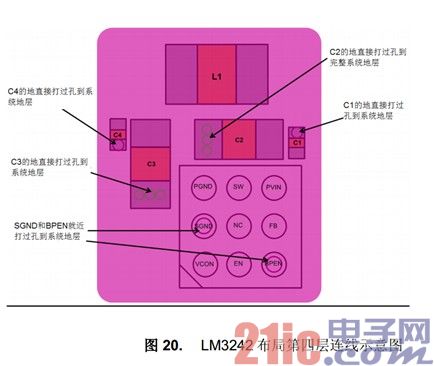
The fourth layer: the system ground layer, which requires a layer of complete copper foil as the ground plane, which can be used as a common connection ground for the chip SGND/PGND.
11 Conclusions and mainstream RF power amplifier power products
Today's handheld devices are becoming more and more versatile, so the challenge is more challenging for the power system design of handheld devices. It is the ultimate goal of power supply design to meet the high performance while maximizing the battery life. SuPA discussed in this paper. The product can effectively save the power consumption of the RF unit, leave valuable energy to other application processors as much as possible, and effectively improve the working time of the equipment. At present, Texas Instruments has produced a series of products to meet the requirements of different RF power amplifiers, such as LM3242. , LM3243, LM3262, LM3263 and support for both boost and buck products for future 4G applications.
12 References
1. LM3242 Technical Manual, Texas Instruments
2. TI AN LM3242 PCB Layout, Texas Instruments
3. 2G-3G-4G RF System Overview, Texas Instruments
Single-axis smartphone stabilizer is a pivoted support that allows the phone staying stabilized.
With a gyro-stabilized gimbal system, it keeps stabilized or steerable horizon with automatic calibration
to give you an unprecedented smooth shooting experience.

1axis smartphone gimbal are designed as pocket size, portable and easy to take.
You can carry it as easy as smartphone!


Wewow focusing on handheld stabilizer is a technology company which does R & D independently.
With Wenpod series product released, the company achieved the industry's praise and quickly became
the leader of the smart stabilizer industry.
Our service
1. Reply to you within 24 hours.
2. Already sample: within 1-2days.
3. Shipping date: within 24 hours once get the payment.
4. 12 months warranty.
5. After-sales service, solve within 3 working dates.
If you have any questions, please contact with us directly.
Wewow appreciates domestic and international business relationship!
Single-axis Smartphone Stabilizer
Single-Axis Smartphone Stabilizer,Professional Single-Axis Smartphone Stabilizer,Smartphone Stabilizer With Single Handheld,Single-Axis Smartphone Gimbal Stabilizer
GUANGZHOU WEWOW ELECTRONIC CO., LTD. , https://www.stabilizers.pl