Platform: XC4VSX55 ​​ISE10.1
Designed the schematic diagram of the FPGA, look at the manual of the FPGA, said the pin assignment problem, such as the clock pin to use the GC class pin, and the single-ended clock input should use the P type pin, can not use the N type pin and many more.
I haven’t tried it all the time, and I’m experimenting with it today for verification.
1) Can GC class global clock pins be used as normal IO?
The so-called GC type pin is a pin with a GC such as IO_L1P_GC_LC in the pin. In fact, the manual says that the GC class pin can be used as the IO, but in the eighth line of the "Xilinx FPGA Development Practical Tutorial" (Tsinghua Press), page 574, the last line says: "All signals input from the global clock pin must be After the IBUF element, otherwise it will report an error when laying out and wiring, so I tried it today and assigned a GC class pin to an ordinary input port (also tested to assign to a common output port). After that, no error occurred.
Therefore, it is concluded that the GC global clock pin can be used as a normal IO. (I don't know if I understand the global clock pin mentioned in the book is wrong, if it is, please don't shoot me, please leave a message)
2) Can non-GC global clock pins be used as clocks?
In fact, as to whether it can be used as a clock, there is another layer of meaning. Of course, if you configure a normal IO port as an input port, you can use its input signal as a clock. That's fine. But we generally don't do this, because the clock signal is a very important signal for us, so the FPGA will have special care inside. If you use the FPGA to pass the reserved clock for the clock and do some processing, then The delay of your clock for various modules is negligible, because the clock is a separate layer when routing, and if you only use normal IO, after the internal layout of the FPGA, from its input, In the place where each clock is used, some lines are long, some lines are short, and its delay will be different. These things still look at the contents of some FPGA structures.
There is a dedicated DCM IP core available in xilinx for execution. Project -> New Source -> IP (CORE Generator & Architecture Wizard) -> FPGA Features and Design -> Clocking -> Virtex- 4——>Single DCM ADV v9.1i, can get the following interface:
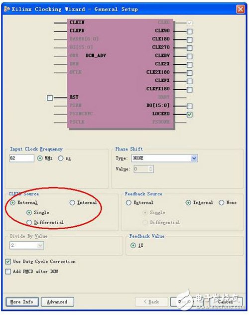
It is important to note that CLKIN Source needs to choose whether it is External or Internal. The source files generated by each are as follows:
========================== Select External======================= ===
`TImescale 1ns / 1ps
Module clk_test(CLKIN_IN,
CLKIN_IBUFG_OUT,
CLK0_OUT,
LOCKED_OUT);
Input CLKIN_IN;
Output CLKIN_IBUFG_OUT;
Output CLK0_OUT;
Output LOCKED_OUT;
Wire CLKFB_IN;
Wire CLKIN_IBUFG;
Wire CLK0_BUF;
Wire GND_BIT;
Wire [6:0] GND_BUS_7;
Wire [15:0] GND_BUS_16;
Assign GND_BIT = 0;
Assign GND_BUS_7 = 7'b0000000;
Assign GND_BUS_16 = 16'b0000000000000000;
Assign CLKIN_IBUFG_OUT = CLKIN_IBUFG;
Assign CLK0_OUT = CLKFB_IN;
IBUFG CLKIN_IBUFG_INST (.I(CLKIN_IN),
.O(CLKIN_IBUFG));
BUFG CLK0_BUFG_INST (.I(CLK0_BUF),
.O(CLKFB_IN));
DCM_ADV DCM_ADV_INST (.CLKFB(CLKFB_IN),
.CLKIN(CLKIN_IBUFG),
.DADDR(GND_BUS_7[6:0]),
.DCLK(GND_BIT),
.DEN(GND_BIT),
.DI(GND_BUS_16[15:0]),
.DWE(GND_BIT),
.PSCLK(GND_BIT),
.PSEN(GND_BIT),
.PSINCDEC(GND_BIT),
.RST(GND_BIT),
.CLKDV(),
.CLKFX(),
.CLKFX180(),
.CLK0(CLK0_BUF),
.CLK2X(),
.CLK2X180(),
.CLK90(),
.CLK180(),
.CLK270(),
.DO(),
.DRDY(),
.LOCKED(LOCKED_OUT),
.PSDONE());
Defparam DCM_ADV_INST.CLK_FEEDBACK = "1X";
Defparam DCM_ADV_INST.CLKDV_DIVIDE = 2.0;
Defparam DCM_ADV_INST.CLKFX_DIVIDE = 1;
Defparam DCM_ADV_INST.CLKFX_MULTIPLY = 4;
Defparam DCM_ADV_INST.CLKIN_DIVIDE_BY_2 = "FALSE";
Defparam DCM_ADV_INST.CLKIN_PERIOD = 16.129;
Defparam DCM_ADV_INST.CLKOUT_PHASE_SHIFT = "NONE";
Defparam DCM_ADV_INST.DCM_AUTOCALIBRATION = "TRUE";
Defparam DCM_ADV_INST.DCM_PERFORMANCE_MODE = "MAX_SPEED";
Defparam DCM_ADV_INST.DESKEW_ADJUST = "SYSTEM_SYNCHRONOUS";
Defparam DCM_ADV_INST.DFS_FREQUENCY_MODE = "LOW";
Defparam DCM_ADV_INST.DLL_FREQUENCY_MODE = "LOW";
Defparam DCM_ADV_INST.DUTY_CYCLE_CORRECTION = "TRUE";
Defparam DCM_ADV_INST.FACTORY_JF = 16'hF0F0;
Defparam DCM_ADV_INST.PHASE_SHIFT = 0;
Defparam DCM_ADV_INST.STARTUP_WAIT = "FALSE";
Endmodule
=========================== Select Internal======================= ===
`timescale 1ns / 1ps
Module clk1_test(CLKIN_IN,
CLK0_OUT,
LOCKED_OUT);
Input CLKIN_IN;
Output CLK0_OUT;
Output LOCKED_OUT;
Wire CLKFB_IN;
Wire CLK0_BUF;
Wire GND_BIT;
Wire [6:0] GND_BUS_7;
Wire [15:0] GND_BUS_16;
Assign GND_BIT = 0;
Assign GND_BUS_7 = 7'b0000000;
Assign GND_BUS_16 = 16'b0000000000000000;
Assign CLK0_OUT = CLKFB_IN;
BUFG CLK0_BUFG_INST (.I(CLK0_BUF),
.O(CLKFB_IN));
DCM_ADV DCM_ADV_INST (.CLKFB(CLKFB_IN),
.CLKIN(CLKIN_IN),
.DADDR(GND_BUS_7[6:0]),
.DCLK(GND_BIT),
.DEN(GND_BIT),
.DI(GND_BUS_16[15:0]),
.DWE(GND_BIT),
.PSCLK(GND_BIT),
.PSEN(GND_BIT),
.PSINCDEC(GND_BIT),
.RST(GND_BIT),
.CLKDV(),
.CLKFX(),
.CLKFX180(),
.CLK0(CLK0_BUF),
.CLK2X(),
.CLK2X180(),
.CLK90(),
.CLK180(),
.CLK270(),
.DO(),
.DRDY(),
.LOCKED(LOCKED_OUT),
.PSDONE());
Defparam DCM_ADV_INST.CLK_FEEDBACK = "1X";
Defparam DCM_ADV_INST.CLKDV_DIVIDE = 2.0;
Defparam DCM_ADV_INST.CLKFX_DIVIDE = 1;
Defparam DCM_ADV_INST.CLKFX_MULTIPLY = 4;
Defparam DCM_ADV_INST.CLKIN_DIVIDE_BY_2 = "FALSE";
Defparam DCM_ADV_INST.CLKIN_PERIOD = 16.129;
Defparam DCM_ADV_INST.CLKOUT_PHASE_SHIFT = "NONE";
Defparam DCM_ADV_INST.DCM_AUTOCALIBRATION = "TRUE";
Defparam DCM_ADV_INST.DCM_PERFORMANCE_MODE = "MAX_SPEED";
Defparam DCM_ADV_INST.DESKEW_ADJUST = "SYSTEM_SYNCHRONOUS";
Defparam DCM_ADV_INST.DFS_FREQUENCY_MODE = "LOW";
Defparam DCM_ADV_INST.DLL_FREQUENCY_MODE = "LOW";
Defparam DCM_ADV_INST.DUTY_CYCLE_CORRECTION = "TRUE";
Defparam DCM_ADV_INST.FACTORY_JF = 16'hF0F0;
Defparam DCM_ADV_INST.PHASE_SHIFT = 0;
Defparam DCM_ADV_INST.STARTUP_WAIT = "FALSE";
Endmodule
Compare the above two pieces of code, the difference is that when the selection is External, CLKIN passes through IBUFG to DCM_ADV, and the internal CLKIN selects directly to DCM_AV, and IBUFG is the primitive "global clock buffer" unit. We use External when we use it. Only when we cascade two DCM modules, directly select External from the outside and the other select Internal.
This is also a point of knowledge in this article: when two DCMs are cascaded, the External is directly connected to the outside, and the other is Internal.
So the subject of this paragraph is "Can non-GC global clock pins be used for clocking?" In fact, more should be referred to "Can non-GC global clock pins be connected to IBUFG?"
In the experiment, we configured the input CLKIN input pin of the External DCM as a normal IO port, that is, the non-GC type global clock pin. The following errors occurred during the place and route phase:
ERROR:Place:645 - A clock IOB clock component is not placed at an optimal clock IOB site. The clock IOB component
Therefore, it is concluded that non-GC global clock pins can not be used as clocks (in fact, they cannot be connected to the input of IBUFG).
3) As mentioned in the Xilinx manual, if a single-ended input clock is used, and a P-type GC global clock pin is used, is the space N type of pin available?
The so-called P type or N type actually refers to IO_L1P_GC_LC or IO_L1N_GC_LC, pay attention to L1P and L1N here, which indicates whether this pin is P type or N type.
In the experiment, we configured the N-type global clock pin to CLKIN. As a result, the same error as in (2) occurred during layout.
Therefore, it is concluded that the GC type global clock pin N type pin can not be used as a single-ended clock input pin (in fact, it cannot be used as the input of IBUFG).
4) Can the differential clock input clock pin be configured with normal IO? The N type pin and the P type pin must be configured with the P type GC global clock pin and the N type GC global clock pin respectively.
<4.1> A pair of normal IO configurations are used for the CLKIN_N_IN and CLKIN_P_IN of the DCM, and the P type of the normal IO is assigned to the CLKIN_N_IN type input of the DCM, and the N type of the IO is assigned to the CLKIN_P_IN type input of the DCM, and the following error occurs. :
ERROR: Place: 604 - The I/O components "clkp" and "clkn" are the P- and N-sides of a differental I/O pair. The component
<4.2> A pair of normal IO configurations are used for the CLKIN_N_IN and CLKIN_P_IN of the DCM, and the P type of the normal IO is correspondingly assigned to the CLKIN_P_IN type input of the DCM, and the N type of the IO is assigned to the CLKIN_N_IN type input of the DCM. The following error:
ERROR:Place:645 - A clock IOB clock component is not placed at an optimal clock IOB site. The clock IOB component
<4.3> Use a pair of GC-type global clock IO pins to configure CLKIN_N_IN and CLKIN_P_IN for DCM, and assign the P type of the normal IO to the CLKIN_N_IN type input of DCM, and the N type of IO is assigned to the CLKIN_P_IN type input of DCM. , the same error as in 4.1.
<4.4> Normal configuration, that is, a pair of GC-type global clock IO pins are used to configure CLKIN_N_IN and CLKIN_P_IN for DCM, and the P-type of the common IO is correspondingly assigned to the CLKIN_P_IN type input of DCM, and the N type of IO The CLKIN_N_IN type input assigned to the DCM is completely correct.
Therefore, it is concluded that the differential clock input must be configured with a pair of GC-type global clock IO pins to the DCCM's CLKIN_N_IN and CLKIN_P_IN, and the N type and P type must match.
In fact, this is the original IBUFGDS in the end, look at the original file of the differential input DCM:
IBUFGDS CLKIN_IBUFGDS_INST (.I(CLKIN_P_IN),
.IB(CLKIN_N_IN),
.O(CLKIN_IBUFGDS));
5) What if the input and output ports are configured as non-IO pins?
In the experiment, a VCCO was configured to be given to the output port, and the result was the following error during the mapping phase:
ERROR: MapLib:30 - LOC constraint AF17 on q<2> is invalid: No such site on the
Therefore, the input and output ports cannot be configured as non-IO pins, and of course the configuration itself is unreasonable.
Original projector bulb lamp is imported from the original brand factory, and the quality is worthy of assurance. At the same time, it has high brightness and durable life, which can present a relatively clear image. It is suitable for places with high requirements for product quality, such as movie theaters, golf courses, schools, etc.
Original Bulb Lamp, Machine Bulbs,Bulb Lampfor Projector,Overhead Projector Bulb
Shenzhen Happybate Trading Co.,LTD , https://www.happybateprojector.com