Abstract: The following arTIcle provides an insight into the features and funcTIonality of Maxim's new LO buffer / splitter family MAX9987 and MAX9990. The paper covers specified parameters and their importance and impact on system applicaTIons such as cellular basestaTIons and concludes with practical applications circuits, which configure the buffer / splitter circuits to adjust output power levels analog and digital as well as compensate for temperature fluctuations.
IntroductionIn today's competitive market, wireless basestation designers are faced with the daunting task of driving down product costs while maintaining superior levels of radio performance. Cost can be cut by reducing DM (direct material) expenditures, part count, design time, variability in performance, and by designing out system failures. At the same time, cellular operators are demanding higher density systems which pack two to four times as much hardware into the footprint of current basestations.
A common solution is to employ greater degrees of circuit integration throughout the receive and transmit lineups. The MAX9987 / MAX9990 family of LO buffers / splitters have been designed with this goal in mind. These components improve the performance of the LO drive lineup by offering exceptional POUT variance control, isolation, and noise performance-all critical parameters for optimizing passive mixer designs.
An overview of typical LO drive circuits is provided below, with a description of how the MAX9987 / MAX9990 family of parts can be optimized for virtually any LO drive application.
Challenges Associated with LO Drive DesignsA typical LO lineup requires a buffer amplifier to isolate and drive a passive mixer from a VCO with relatively low output power. Most passive mixers require drive levels ranging from + 14dBm to + 20dBm. However, simple amplification of the VCO signal is not sufficient for optimizing mixer performance. A key requirement for any LO lineup is to maintain a nominal drive level despite temperature, voltage and VCO drive variations. Failure to contain LO drive variance can lead to degradations in receiver sensitivity and IP3 performance. For the transmit chain, LO drive variance can also impact output power, IP3 and corresponding ACPR.
Most of the variance encountered within an LO drive circuit is directly related to the VCO's output characteristics. The output power of a VCO can typically vary by as much as ± 3dB, depending upon temperature, frequency and part-to-part differences. Table 1 provides a detailed look at each of these variance contributors.
Table 1. Contributing Factors to VCO Output Power Variance
As shown, VCO part-to-part differences are the most significant contributors to power variance in the LO drive circuit. However, a good LO drive circuit attempts to address all of the variances with one common solution. Traditional SolutionsDiscrete solutions are typically used in today's high power diversity and single branch LO drive circuits (see Figure 1). The overwhelming majority of these circuits use at least one amplifier that is driven hard into saturation. By pushing the amp (s) into compression, a relatively stable level of output drive is provided regardless of variations in PIN, temperature and supply voltage.
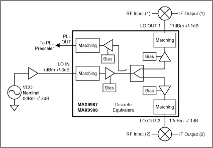
Figure 1. Typical application circuit using the MAX9987 / MAX9988 LO buffers / splitters.
However, the drawback of these discrete solutions is that they are relatively bulky, especially when a designer uses lumped or distributed Wilkinson splitters as the representation of the power divider. Also, the part count can be significant as noted in Table 2.
Table 2. MAX9987 / MAX9988 Size, Part Count and Cost Comparison
The MAX9987 / MAX9990 AlternativeAs shown in Figure 1, the MAX9987 / MAX9988 replaces four discrete amplifiers, a passive splitter and coupler, plus dozens of biasing components. This high degree of integration enables a designer to reduce the overall size of the LO drive circuitry by a factor of 2.5x, while simultaneously cutting part count by as much as 41%. Table 2 provides a more detailed look at how well this part stacks up against its discrete equivalent.
These components are ideal for cellular / GSM / DCS / PCS and UMTS basestation applications where dual, high level LO drives are required for diversity transmit and receive lineups. Single output versions, namely the MAX9989 / MAX9990, can be similarly used for single branch systems . At the heart of each device is the on-chip buffer circuit, which provides an output to input isolation of 40dB to prevent LO pulling, and an output-to-output isolation of 30dB to reduce branch-to-branch interference. As an added benefit, the MAX9987 / MAX9990 feature an on-board PLL amplifier which provides a convenient + 3dBm output for prescaler feedback. Each member of the MAX9987 / MAX9990 family comes in a remarkably small, pin-compatible 5mm x 5mm QFN-20 package.
Using the MAX9987 / MAX9990 in its Standard ConfigurationThe MAX9987–MAX9990 series of LO buffers / splitters were specifically designed to provide LO drive control of better than ± 1dB over temperature (-40 ° C to + 85 ° C), PIN (± 3dB) and VSUPPLY (5 ± 0.25V); all without the use of external calibration or control.
Figure 2 depicts the basic relationship between POUT and PIN for the MAX9987 / MAX9990's typical application circuit. As shown, the device is capable of providing ± 1dB variance control over a relatively large PIN swing of ± 3dB. The designer is tasked with providing a nominal level of PIN for the MAX9987 / MAX9990. After this nominal level is determined, all variance control, including part-to-part variations, is handled directly by the IC.
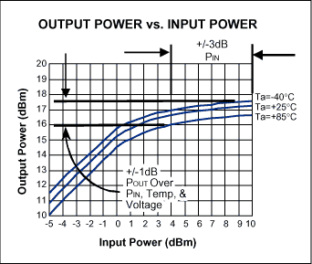
Figure 2. MAX9987 / MAX9990 output power characteristics using the typical application circuit (nominal POUT set for + 17dBm).
A nominal output level of + 17dBm is shown in Figure 2. Note, however, that the MAX9987 / MAX9990 also possess a feature whereby the designer can precision-set the output power levels through the implementation of four external biasing resistors. In effect, these resistors determine the degree of biasing on the chip's internal amplifiers. The specified output power levels are adjustable from + 14dBm to + 20dBm, depending upon the chosen resistor settings. (Refer to Figure 3; the MAX9987 / MAX9990 data sheets can also provide additional details ).
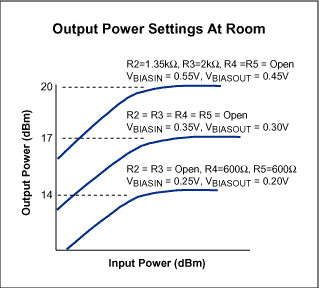
Figure 3. POUT level control using the MAX9987 / MAX9990's biasing feature.
Utilizing the MAX9987 / MAX9990's Biasing Feature to Compensate for Part-to-Part Variations in LO Drive CircuitsFor the majority of LO drive applications, ± 1dB of variance control is more than sufficient for optimizing mixer performance. However, in certain cases, a designer may find it desirable to limit this variance to even lower limits.
The technique presented below caters to such an application by extending the capabilities of the MAX9987 / MAX9990 to yield nominal output levels that are accurate to within 0.05dB. Such adjustments allow the designer to calibrate out part-to-part differences which lead to variances in input drive level. In the case of a typical LO drive circuit, the VCO's part-to-part variations of ± 2dB can be eliminated altogether. All that remains is a very managable delta of less than ± 0.5dB over temperature and voltage, centered around the calibrated value of POUT.
The calibration process is facilitated by the MAX9987 / MAX9990's programmable POUT feature. Instead of using fixed resistors, it is possible to control the output power directly with a voltage applied to the reference pins. This type of control provides the option of modifying the output power at any time, and lends itself to dynamic adjustments which can be implemented during a calibration test. The proposed method, shown in Figure 4, allows for testing and setting of the output power level in a production environment. Other possible implementations are suggested towards the the end of this article.
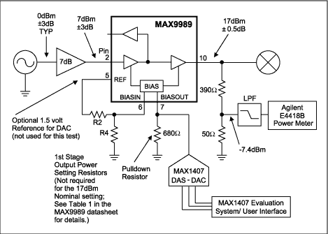
Figure 4. RF sense and DAC power control circuit for the MAX9989 / MAX9990 (single output versions).
For demonstrative purposes, the goal of the design shown in Figure 4 is to set (with high accuracy) an output power level of 17dBm on the MAX9989. Other output power levels are possible, depending upon the level of bias applied to the reference pin. In addition, this technique can be applied to any member of the MAX9987 / MAX9990 family.
For the bench test of this circuit implementation, a constant + 7dBm RF source at 900MHz was used to drive the MAX9989. Figure 5 shows the measured transfer function of RF output vs. DAC voltage for this particular circuit. Lab measurements of this circuit reveal that the output power of the MAX9989 can be fine-tuned with 0.05dB accuracy. It should be noted that for this particular circuit, a nominal level of 17dBm (delivered to the load) corresponds to a DAC voltage of 320mV. The coupler used on the calibration port taps off -7.4dBm of power from the MAX9989, and hence the designer needs to drive the bias on the device a bit higher to compensate for the 0.3dB coupler loss.
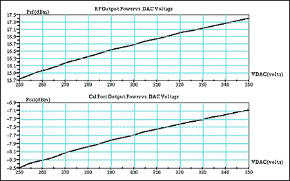
Figure 5. Measured RF power vs. control voltage for the MAX9989.
The following lists some key findings from the implementation presented in Figure 4:
DAC Selection: If a 10-bit DAC is used to set a voltage between 0 and 1.25V, the control resolution will be:
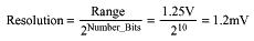
Control is approximately 0.02dB / mV, so the resolution is effectively 0.02dB (which is more than sufficient for our target of 0.05dB control). It is possible to use an 8-bit DAC to provide sufficient resolution, depending on the goal of the application. For measurement simplicity, the plots shown in Figure 5 were generated using a DAC integrated within the MAX1407 (a data acqusition system on a chip). Other standalone DACs, such as the 2-channel, 3-wire interface, 8- bit MAX519, are suitable for this type of control as well.
Reference for DAC: The MAX1407 used in Figure 4 has an internal reference at 1.25V which is used for Maxim's internal testing. If anther DAC is used, it is possible to utilize the MAX9989's internal 1.5V reference source (available on pin 5 of the device).
Low-Pass Filter: A low-pass filter is used to reject any 2nd or higher-order harmonic component that is generated from the saturated amplifier. When measuring the load RF power directly a low-pass filter should be used as well. In this case a 1200MHz coaxial filter was used. Additional VariantsFurther enhancements to the circuit in Figure 4 are also possible; four additional possibilities are presented below:
Setting the Output Power to Levels Other than 17dBm: A designer may wish to precision set the output power to a level between +14 and + 17dBm. To do so, connect pin 6 (BIASIN) to the resistors R2 and R4 shown in Figure 4 . Suggested values ​​of R2 and R4 are provided in Table 1 of the MAX9989 data sheet.
Wide Range Power Variations: It may be of interest to adjust the MAX9987 / MAX9990's power level over a wide range, rather than for precision setting at a specific level. As noted above, the device's output power level is adjustable from +14 to + 20dBm . DAC control can be used to realize these output power levels with user control. To extend the control range, it is suggested that the bias voltages on both pins 6 and 7 are raised or lowered, rather than the bias on just pin 7. Since each pin will require different biases, it is recommended that the designer use two separate DACs in this implementation. Refer to Figure 3 for details on the ideal voltages applied to pins 6 and 7.
Temperature Control: The amount of POUT variance can be reduced even further if the designer can account for changes in ambient temperature. As shown in Figures 6 and 7, it is possible to link a temperature sensor to the bias control of the MAX9989. A positive or negative temperature slope could be implemented, allowing the user to set the power / temperature profile to extract the best qualities of the following RF stage.
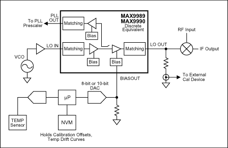
Figure 6. Temperature compensation using a digital technique.
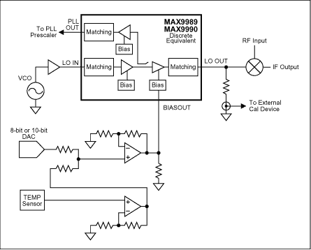
Figure 7. Temperature compensation using an analog technique.
Real Time Closed Control Loop: A closed loop control system can be employed for even greater accuracy. Figure 8 represents one possible implementation using an analog integration circuit.
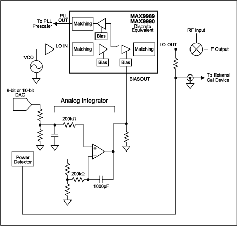
Figure 8. Analog closed loop control.
ConclusionRegardless of their implementation, the MAX9987 / MAX9990 are ideal parts for providing high levels of LO drive with exceptional POUT variance control. By using these devices, basestation designers can dramatically improve the performance of their LO drive circuit while only using a fraction of their current component count and board footprint. These advances will help designers meet the increasing demands of today's basestation operators.
A similar version of this article appeared in the February 2003 issue of Microwaves & RF magazine.
IntroductionIn today's competitive market, wireless basestation designers are faced with the daunting task of driving down product costs while maintaining superior levels of radio performance. Cost can be cut by reducing DM (direct material) expenditures, part count, design time, variability in performance, and by designing out system failures. At the same time, cellular operators are demanding higher density systems which pack two to four times as much hardware into the footprint of current basestations.
A common solution is to employ greater degrees of circuit integration throughout the receive and transmit lineups. The MAX9987 / MAX9990 family of LO buffers / splitters have been designed with this goal in mind. These components improve the performance of the LO drive lineup by offering exceptional POUT variance control, isolation, and noise performance-all critical parameters for optimizing passive mixer designs.
An overview of typical LO drive circuits is provided below, with a description of how the MAX9987 / MAX9990 family of parts can be optimized for virtually any LO drive application.
Challenges Associated with LO Drive DesignsA typical LO lineup requires a buffer amplifier to isolate and drive a passive mixer from a VCO with relatively low output power. Most passive mixers require drive levels ranging from + 14dBm to + 20dBm. However, simple amplification of the VCO signal is not sufficient for optimizing mixer performance. A key requirement for any LO lineup is to maintain a nominal drive level despite temperature, voltage and VCO drive variations. Failure to contain LO drive variance can lead to degradations in receiver sensitivity and IP3 performance. For the transmit chain, LO drive variance can also impact output power, IP3 and corresponding ACPR.
Most of the variance encountered within an LO drive circuit is directly related to the VCO's output characteristics. The output power of a VCO can typically vary by as much as ± 3dB, depending upon temperature, frequency and part-to-part differences. Table 1 provides a detailed look at each of these variance contributors.
Table 1. Contributing Factors to VCO Output Power Variance
| Parameter | Parameter Range | Typical Power Variance |
| Temperature | -40 ° C to + 85 ° C | ± 0.5dB to ± 1dB |
| Frequency | ± 30MHz | ± 0.5dB to ± 1dB |
| Part-to-Part Difference | ± 1dB to ± 2dB | |
| Total Variance | Over temperature, frequency and component-to-component | ± 2dB to ± 3dB |
As shown, VCO part-to-part differences are the most significant contributors to power variance in the LO drive circuit. However, a good LO drive circuit attempts to address all of the variances with one common solution. Traditional SolutionsDiscrete solutions are typically used in today's high power diversity and single branch LO drive circuits (see Figure 1). The overwhelming majority of these circuits use at least one amplifier that is driven hard into saturation. By pushing the amp (s) into compression, a relatively stable level of output drive is provided regardless of variations in PIN, temperature and supply voltage.
Figure 1. Typical application circuit using the MAX9987 / MAX9988 LO buffers / splitters.
However, the drawback of these discrete solutions is that they are relatively bulky, especially when a designer uses lumped or distributed Wilkinson splitters as the representation of the power divider. Also, the part count can be significant as noted in Table 2.
Table 2. MAX9987 / MAX9988 Size, Part Count and Cost Comparison
| Component | Maxim Part Count | Competing Solution Part Count | Space Per Part (mm²) | Space for Maxim Solution (mm²) | Space for Competing Solution (mm²) | Average Cost per Part | Maxim Cost | Competing Solution Cost | Cost Savings |
| C | 14 | 16 | 3.75 | 52.5 | 60 | $ 0.01 | $ 0.14 | $ 0.16 | $ 0.02 |
| L | 0 | 9 | 7.7 | 0 | 69.3 | $ 0.04 | $ 0.00 | $ 0.36 | $ 0.36 |
| R | 5 | 4 | 3.75 | 18.75 | 15 | $ 0.005 | $ 0.03 | $ 0.02 | -$ 0.01 |
| Amps | 0 | 4 | 18.5 | 0 | 74 | $ 1.10 | $ 0.00 | $ 4.40 | $ 4.40 |
| Splitter | 0 | 1 | 31 | 0 | 31 | $ 1.25 | $ 0.00 | $ 1.25 | $ 1.25 |
| MAX9987 / MAX9988 | 1 | 0 | 25 | 25 | 0 | ||||
| Total | 20 | 34 | 96.25 | 249.3 | $ 6.03 |
The MAX9987 / MAX9990 AlternativeAs shown in Figure 1, the MAX9987 / MAX9988 replaces four discrete amplifiers, a passive splitter and coupler, plus dozens of biasing components. This high degree of integration enables a designer to reduce the overall size of the LO drive circuitry by a factor of 2.5x, while simultaneously cutting part count by as much as 41%. Table 2 provides a more detailed look at how well this part stacks up against its discrete equivalent.
These components are ideal for cellular / GSM / DCS / PCS and UMTS basestation applications where dual, high level LO drives are required for diversity transmit and receive lineups. Single output versions, namely the MAX9989 / MAX9990, can be similarly used for single branch systems . At the heart of each device is the on-chip buffer circuit, which provides an output to input isolation of 40dB to prevent LO pulling, and an output-to-output isolation of 30dB to reduce branch-to-branch interference. As an added benefit, the MAX9987 / MAX9990 feature an on-board PLL amplifier which provides a convenient + 3dBm output for prescaler feedback. Each member of the MAX9987 / MAX9990 family comes in a remarkably small, pin-compatible 5mm x 5mm QFN-20 package.
Using the MAX9987 / MAX9990 in its Standard ConfigurationThe MAX9987–MAX9990 series of LO buffers / splitters were specifically designed to provide LO drive control of better than ± 1dB over temperature (-40 ° C to + 85 ° C), PIN (± 3dB) and VSUPPLY (5 ± 0.25V); all without the use of external calibration or control.
Figure 2 depicts the basic relationship between POUT and PIN for the MAX9987 / MAX9990's typical application circuit. As shown, the device is capable of providing ± 1dB variance control over a relatively large PIN swing of ± 3dB. The designer is tasked with providing a nominal level of PIN for the MAX9987 / MAX9990. After this nominal level is determined, all variance control, including part-to-part variations, is handled directly by the IC.
Figure 2. MAX9987 / MAX9990 output power characteristics using the typical application circuit (nominal POUT set for + 17dBm).
A nominal output level of + 17dBm is shown in Figure 2. Note, however, that the MAX9987 / MAX9990 also possess a feature whereby the designer can precision-set the output power levels through the implementation of four external biasing resistors. In effect, these resistors determine the degree of biasing on the chip's internal amplifiers. The specified output power levels are adjustable from + 14dBm to + 20dBm, depending upon the chosen resistor settings. (Refer to Figure 3; the MAX9987 / MAX9990 data sheets can also provide additional details ).
Figure 3. POUT level control using the MAX9987 / MAX9990's biasing feature.
Utilizing the MAX9987 / MAX9990's Biasing Feature to Compensate for Part-to-Part Variations in LO Drive CircuitsFor the majority of LO drive applications, ± 1dB of variance control is more than sufficient for optimizing mixer performance. However, in certain cases, a designer may find it desirable to limit this variance to even lower limits.
The technique presented below caters to such an application by extending the capabilities of the MAX9987 / MAX9990 to yield nominal output levels that are accurate to within 0.05dB. Such adjustments allow the designer to calibrate out part-to-part differences which lead to variances in input drive level. In the case of a typical LO drive circuit, the VCO's part-to-part variations of ± 2dB can be eliminated altogether. All that remains is a very managable delta of less than ± 0.5dB over temperature and voltage, centered around the calibrated value of POUT.
The calibration process is facilitated by the MAX9987 / MAX9990's programmable POUT feature. Instead of using fixed resistors, it is possible to control the output power directly with a voltage applied to the reference pins. This type of control provides the option of modifying the output power at any time, and lends itself to dynamic adjustments which can be implemented during a calibration test. The proposed method, shown in Figure 4, allows for testing and setting of the output power level in a production environment. Other possible implementations are suggested towards the the end of this article.
Figure 4. RF sense and DAC power control circuit for the MAX9989 / MAX9990 (single output versions).
For demonstrative purposes, the goal of the design shown in Figure 4 is to set (with high accuracy) an output power level of 17dBm on the MAX9989. Other output power levels are possible, depending upon the level of bias applied to the reference pin. In addition, this technique can be applied to any member of the MAX9987 / MAX9990 family.
For the bench test of this circuit implementation, a constant + 7dBm RF source at 900MHz was used to drive the MAX9989. Figure 5 shows the measured transfer function of RF output vs. DAC voltage for this particular circuit. Lab measurements of this circuit reveal that the output power of the MAX9989 can be fine-tuned with 0.05dB accuracy. It should be noted that for this particular circuit, a nominal level of 17dBm (delivered to the load) corresponds to a DAC voltage of 320mV. The coupler used on the calibration port taps off -7.4dBm of power from the MAX9989, and hence the designer needs to drive the bias on the device a bit higher to compensate for the 0.3dB coupler loss.
Figure 5. Measured RF power vs. control voltage for the MAX9989.
The following lists some key findings from the implementation presented in Figure 4:
DAC Selection: If a 10-bit DAC is used to set a voltage between 0 and 1.25V, the control resolution will be:
Control is approximately 0.02dB / mV, so the resolution is effectively 0.02dB (which is more than sufficient for our target of 0.05dB control). It is possible to use an 8-bit DAC to provide sufficient resolution, depending on the goal of the application. For measurement simplicity, the plots shown in Figure 5 were generated using a DAC integrated within the MAX1407 (a data acqusition system on a chip). Other standalone DACs, such as the 2-channel, 3-wire interface, 8- bit MAX519, are suitable for this type of control as well.
Reference for DAC: The MAX1407 used in Figure 4 has an internal reference at 1.25V which is used for Maxim's internal testing. If anther DAC is used, it is possible to utilize the MAX9989's internal 1.5V reference source (available on pin 5 of the device).
Low-Pass Filter: A low-pass filter is used to reject any 2nd or higher-order harmonic component that is generated from the saturated amplifier. When measuring the load RF power directly a low-pass filter should be used as well. In this case a 1200MHz coaxial filter was used. Additional VariantsFurther enhancements to the circuit in Figure 4 are also possible; four additional possibilities are presented below:
Setting the Output Power to Levels Other than 17dBm: A designer may wish to precision set the output power to a level between +14 and + 17dBm. To do so, connect pin 6 (BIASIN) to the resistors R2 and R4 shown in Figure 4 . Suggested values ​​of R2 and R4 are provided in Table 1 of the MAX9989 data sheet.
Wide Range Power Variations: It may be of interest to adjust the MAX9987 / MAX9990's power level over a wide range, rather than for precision setting at a specific level. As noted above, the device's output power level is adjustable from +14 to + 20dBm . DAC control can be used to realize these output power levels with user control. To extend the control range, it is suggested that the bias voltages on both pins 6 and 7 are raised or lowered, rather than the bias on just pin 7. Since each pin will require different biases, it is recommended that the designer use two separate DACs in this implementation. Refer to Figure 3 for details on the ideal voltages applied to pins 6 and 7.
Temperature Control: The amount of POUT variance can be reduced even further if the designer can account for changes in ambient temperature. As shown in Figures 6 and 7, it is possible to link a temperature sensor to the bias control of the MAX9989. A positive or negative temperature slope could be implemented, allowing the user to set the power / temperature profile to extract the best qualities of the following RF stage.
Figure 6. Temperature compensation using a digital technique.
Figure 7. Temperature compensation using an analog technique.
Real Time Closed Control Loop: A closed loop control system can be employed for even greater accuracy. Figure 8 represents one possible implementation using an analog integration circuit.
Figure 8. Analog closed loop control.
ConclusionRegardless of their implementation, the MAX9987 / MAX9990 are ideal parts for providing high levels of LO drive with exceptional POUT variance control. By using these devices, basestation designers can dramatically improve the performance of their LO drive circuit while only using a fraction of their current component count and board footprint. These advances will help designers meet the increasing demands of today's basestation operators.
A similar version of this article appeared in the February 2003 issue of Microwaves & RF magazine.
Brushless BLDC Worm Gear Motors
Worm Gear Motor,Planetary Gear Motor,Brushless Gear Motor,Brushless Bldc Worm Gear Motors
Jinan Keya Electron Science And Technology Co., Ltd. , https://www.keyaservo.com