Large-scale RF integration reduces mobile phone board area and power consumption
In today's wireless equipment, more than half of the components on the circuit board are analog RF devices, so an effective way to reduce the board area and power consumption is to conduct larger-scale RF integration and develop toward system-level chips. This article introduces the current status of RF integration development, and proposes countermeasures and solutions to some of these problems.
A few years ago, the cellular phone market was still dominated by single-band and dual-band single-mode phones. The technology used only supported one or two cellular frequency bands, using the same modulation method, multiple access scheme and protocol in all supported frequency bands. . In comparison, today ’s new-generation cellular phones are much more complex in design, can provide multi-band, multi-mode support, have Bluetooth personal area network, GPS positioning and other functions, and ultra-wideband and TV reception functions have begun to appear, in addition to Applications such as games, images, audio and video have also become very common in mobile phones.
The wireless phone is becoming such a complicated device as a so-called handheld personal entertainment center, and its development trend continues to bring more challenges to designers. Although compared to voice-only phones, the new generation of mobile phones have increased significantly in terms of communication processing, application processing, number of RF interfaces, and integrated memory capacity, but users still expect mobile phones to have a smaller size and a streamlined shape. And low price, but also have a large color display that can provide standby and talk time similar to traditional voice mobile phones. Maintaining the existing form factor and power consumption while increasing the function exponentially, while maintaining the overall system cost unchanged, these pose a lot of problems for system designers.
Obviously, the problem involves various parts of the overall system design, as well as all wireless communication and entertainment content providers. One area that is particularly effective in reducing board area and power consumption is the RF part of wireless system design. This is because in today's typical mobile phones, more than half of the components on the board are analog RF components. These components are added to Together they occupy 30 to 40% of the entire circuit board area, and the addition of radio frequency systems such as Bluetooth, GPS and WLAN will also greatly increase the space requirements.
The solution is to conduct larger-scale RF integration and eventually develop into a fully integrated system-on-chip. Some designers put the analog-to-digital converter in the antenna to reduce the total circuit board space required for RF functions. When semiconductor integration technology can integrate more functions in a single device, the number of discrete devices and used to accommodate these devices The board space is reduced accordingly. As the industry moves toward system-on-chip integration, designers will continue to discover new technologies to meet the contradiction between higher RF complexity and extended battery life in small wireless devices.
RF integration development status An important development of RF integration occurred about three years ago, when the development of RF technology and digital baseband modems made it possible to replace superheterodyne RF devices with direct down-conversion receivers in wireless handsets. Superheterodyne RF devices use multi-stage mixers, filters, and multiple voltage-controlled oscillators (VCOs). They have been well used for many years, but the integration of direct conversion RF devices can greatly reduce the overall number of GSM RF components. In the late 1990s, a typical single-band superheterodyne RF subsystem including PA, antenna switch, LDO, small-signal RF, and VCTCXO required approximately 200 discrete devices; today, we can design a four-band function The direct conversion system of the company integrates VCO, VCXO and PLL loop filter, but its number of components is less than 50.
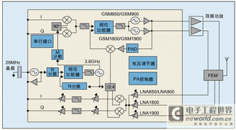
For example, the Texas Instruments transceiver TRF6151 for GSM (Figure 1), the integrated functions include on-chip voltage regulator, VCO and VCO tank, PA power control, PLL loop filter EDGE blocker detection, LNA gain step control And VCXO.
For designers, advanced integration helps to overcome some of the big problems in wireless RF, the most basic of which is the DC power supply of the transceiver and its regulation. During a call, as the temperature and time change, the battery voltage will change. In addition, the noise coupling from the TX VCO and RX VCO power supply will also affect the performance of the entire system, so designers are faced with how to solve the RF circuit board regulator and large Most issues related to passive components. Integrating these devices in the RF transceiver means that the only external components required are simple decoupling capacitors. This direct connection to the power supply not only simplifies the design, but also saves board space.
Another challenge facing RF designers is the VCO tuning range and lock time. In all analog VCO designs. Because it is often necessary to balance the lock time and tuning range, the loop filter is generally placed outside the chip. Sometimes, this can be solved in the software control of the VCO tuning range, but this method puts additional resource requirements on the overall development of the phone. When the digital tuning function is included in the VCO and can provide self-calibration, you can get an extended tuning range, loop filter components can be placed on the chip. Obviously, this solution will allow design engineers to simplify their work.
In order to obtain the transmitter power control required by the GSM system, PA manufacturers generally include this function in the power amplifier module (PAM). The power controller is usually composed of up to several thousand digital CMOS gates, made in a separate chip within PAM, this component will increase the cost of PAM by 0.30 to 0.40 USD. Integrating this function into RF devices will eliminate the need for GaAsPAM manufacturers to purchase digital CMOS circuits and install them in PAM. For an OEM that produces tens of thousands of products per month, removing this extra component will greatly reduce Their cost.
Another area where advanced integration can bring substantial savings is VCXO. In the past, it was necessary to purchase expensive VCTCXO modules as discrete components designed in RF devices, so incorporating common components of VCTCXO modules into RF devices can reduce costs and related design issues. Using TRF6151 requires only a low-priced crystal and variable capacitance The diode can complete the function of VCTCXO.
Despite these integrations and design simplifications, RF design engineers still face difficult choices, one of which is input sensitivity and RX power consumption. As we all know, the larger the current used in the design of a low-noise amplifier (LNA), the lower the overall noise characteristics. The design engineer must determine the total power budget of the receiver and the receiver sensitivity level requirements. But the noise does not decrease as the power decreases, in fact it is the opposite. So although they can meet the GSM standard specifications, designers must often ask themselves whether it is worth the cost of power consumption to achieve a certain sensitivity level. This question also explains why it is necessary for design engineers and IC manufacturers to cooperate closely throughout the design process. The feedback from the design engineers can guide IC manufacturers to better serve the wireless industry when developing future RF products.
The development of SoC to reduce the cost, power and complexity of wireless systems is very important to successfully meet the requirements of system integration. However, the development of high integration solutions for mobile phones requires the semiconductor industry to overcome complex technical obstacles, some of which are rarely designed. People are concerned because many of them do n’t want to know how SoC devices are made, as long as they can provide the required performance. Therefore, it is necessary to have a quick understanding of some process technologies, which will affect the ability and availability of devices used in cellular phone integration.
There are several possible solutions for the integration of mobile phone RF electronic systems. First, you can use traditional technology to implement a traditional RF architecture in a relatively simple bipolar or BiCMOS process. The final RF chip can be assembled with mobile phone digital logic functions using multi-chip packaging technology (system-level packaging technology). Although this technology has many advantages, such as the use of familiar RF design methods and mature processes and technologies, the high cost and limited yield of test devices make it difficult to commercialize.
There is also another method, the integration of mobile phone electronic system can also be obtained by advanced BiCMOS (SiGe) wafer process. However, since the processing of SiGe HBT devices requires additional lithography, the final chip will require an additional cost. At the same time, because SiGe BiCMOS technology cannot use the most advanced lithography process, the BiCMOS process usually lags behind the advanced digital CMOS process. These will bring tremendous pressure to increase the characteristics of mobile phones and reduce costs. It is impossible to solve it with a simple wafer process strategy, because this technology cannot keep the system logic or digital part at the lowest possible price at all times. Monolithic integration of the radio frequency part of the system baseband function in BiCMOS (or SiGe) is not a good choice.
The final solution that can be considered is radio frequency integration in CMOS, which also faces considerable challenges. Although there are several CMOS cellular radio frequency designs, these designs are largely based on analog functions. It is very difficult to implement analog mixers, filters and amplifiers with CMOS technology, and the power consumption is generally greater than that of SiGe BiCMOS. With the development of process technology, the CMOS rated level is getting lower and lower, which makes analog design more difficult. Early in the development of new processes, device modeling and process maturity generally cannot meet the high-precision parameter modeling requirements required for analog module design. However, the recently developed digital CMOS RF architecture makes monolithic CMOS integration more attractive .
As manufacturers seek low-cost RF system-on-chip solutions, these solutions also drive the semiconductor industry forward. Although each integration solution has difficulties, it is indeed surprising that RF component integration can reach such a high level. Overcoming these difficulties will make the design of wireless handsets a big step forward and set the direction for greater integration in the near future.
This article concludes that there are still many difficulties in RF integration. Every RF device of modern mobile phones is facing strict performance requirements, with a sensitivity of about -106dBm (106dB below 1mW) or higher, and the corresponding level is only a few microvolts; in addition, the selectivity is also a useful channel The rejection capability of adjacent frequency bands (often called blocking) should be on the order of 60dB; in addition, the system oscillator is required to operate under very low phase noise to prevent folding blocking energy from entering the receiving band. Because it involves very high frequencies and extremely demanding performance requirements, RF integration is very difficult.
Dealing with multi-frequency standards poses a real challenge for the entire SoC frequency, hoping to mitigate the incentives generated by in-band signal transmission. The integration into digital RF is much more than putting multiple RF components in a single chip There needs to be a new architecture for hardware sharing.
For system designers, current simple, highly integrated, cost-saving semiconductor devices can greatly reduce the design complexity, while at the same time they can enrich the characteristics of wireless devices and keep the system size, battery life and cost unchanged. The new highly integrated RF device can also eliminate some of the debates in wireless design, saving engineers valuable time.
Laser Radar contains LSPD Safety Laser Scanner and LS laser radar. LSPD safety laser scanner is type 3 with CE certificate. It can be used for agv safety and industrial area protection. LS laser radar is for agv guide. Many famous agv manufacturers has installed LS laser radar to guide their agvs. Our cooperating brand contains Quicktron, Mushiny, Aresbots, etc. Feedback from customers are quite posotive.
Laser Radar
Laser Radar,Auto Guided Vehicle Guide Radar,Sick Laser Radar,Safety Scanner,Safety Laser Scanner,Ls Series Laser Radar
Jining KeLi Photoelectronic Industrial Co.,Ltd , https://www.sdkelien.com