Abstract: The first part of this arTIcle series discusses commonly known definiTIons most crucial for high-speed data converters (in this case analog-to-digital converter or short ADCs) used in communicaTIons, instrumentaTIon and data acquisition applications. The purpose of this article is to help the reader gain a better understanding of common parameters such as signal-to-noise ratio (SNR), signal-to-noise-and-distortion (SINAD), total harmonic distortion (THD) and spurious-free dynamic range ( SFDR). In the second part of this article series (see "Dynamic Testing of High-Speed ​​ADCs" for further reading), these parameter definitions are put to the test by measuring them in real-world test scenarios.
Additional Information: Dynamic Testing of High-Speed ​​ADCs, Part 2
Dynamic specifications for ADCs are very important in high-speed applications such as digital communications, ultrasound imaging, instrumentation, and IF digitization. The following discussion provides a definition and a mathematical foundation for each parameter, offers useful techniques for evaluating the dynamic performance of high -speed ADCs, and explains how the dynamic parameters correlate with ADC performance. Part 1 of this two-part discussion covers the definition of these specifications: Signal-to-noise ratio (SNR) Signal-to-noise and distortion ratio (SINAD) Effective number of bits (ENOB) Total harmonic distortion (THD) Spurious-free dynamic range (SFDR) Two-tone intermodulation distortion (TTIMD) Multi-tone intermodulation distortion (MTIMD) Voltage standing-wave ratio (VSWR) In explaining how to measure these parameters, Part 2 provides insight into the practical aspects of dynamic performance testing. Note that some specifications allow more than one approach for measure ment and even for definition. Thus, the test techniques of Part 2 represent one method and are not mandatory. Any of the methods described can be extended or altered as necessary to suit the application at hand.
When testing high-speed A / D converters, one emulates the operation of a spectrum analyzer used to quantify linearity in analog circuits. For this instrument and for the test procedure, dynamic specifications are usually expressed in the frequency domain, using the Fast Fourier Transform (FFT). In both cases, the data output represents the magnitude of this FFT. As an example (Figure 1), consider the FFT plot for an 80Msps, 10-bit ADC designed and optimized for ultrasound imaging and the digitization of baseband / IF frequencies. Such FFT plots contain impressive amounts of information and can be generated quickly. However, to make use of an FFT, one must understand how its parameters are defined.
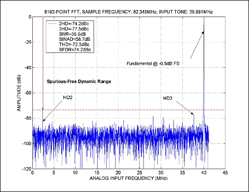
Figure 1. 8192-point FFT plot for the MAX1448.
Signal-to-Noise Ratio (SNR) For a waveform perfectly reconstructed from digital samples, SNR is the ratio of an rms (root mean square) full-scale analog input to its rms quantization error (AQUANTIZATION [rms] = ALSB / √12 = AREF / [2N × √12]). The rms value of a sine wave is one half its peak-to-peak value divided by √2, and quantization error is the difference between an analog waveform and its digitally reconstructed replica, which is characterized by a staircase-shaped transfer curve. The difference function resembles a sawtooth wave that oscillates once per sample between the levels + 1 / 2LSB and -1 / 2LSB (LSB being least-significant bit). The difference function's rms value is its peak value (1 / 2LSB) divided by √3. For an ideal N-bit converter, SNR is defined as SNR-2N × √3 / √2 = 1.23 × 2N. Most of the dynamic specifications are expressed as a ratio of relative measurements rather than absolute units. Thus, the signal-to-noise ratio for an ideal ADC, driven by a full-sca le sinusoidal input with AC power equal to AREF / (2 × √2) in decibels, is SNRdB = 20 × log10 (AIN [rms] / AQUALITIZATION [rms]
SNRdB = 20 × log10 (AREF / [2 × √2] / AREF / [2N × √12])
SNRdB = 6.02 × N + 1.76 SNR is diminished by many noise sources in addition to quantization noise (See Appendix 1). A data converter's resolution and quantization level both help to establish its noise floor. The actual SNR for a sinusoidal input signal can therefore be described as SNRdB = 20 × log10 (ASIGNAL [rms] / ATOTAL_NOISE [rms], where ASIGNAL [rms] represents the rms amplitude for the analog input signal, and ATOTAL_NOISE [rms] is the rms sum of all noise sources (thermal noise , quantization noise, etc.) that limit the converter's dynamic performance. Applying this definition to a 10-bit ADC such as the MAX1448 yields a typical SNR value of 58.4dB at the 40MHz Nyquist frequency (fSAMPLE = 80Msps). This SNR represents 94 % of the ~ 62dB SNR exhibited by an ideal 10-bit ADC.
For an ADC driven by a sinusoidal input with an amplitude equal to the ADC's full-scale input, the maximum theoretical SNR is SNRdB = 6.02 × N + 1.76 + 10 × log10 (fSAMPLE [rms] / 2 × fMAX, where fMAX describes the maximum bandwidth of the input tone, and fSAMPLE is the converter's sampling frequency. From this equation, note that SNR increases as the sampling frequency increases beyond the Nyquist rate (2 × fMAX). Called processing gain, this effect is caused by spreading of the quantization noise power (which is fixed and independent of bandwidth) as the sampling frequency increases. This "oversampling" helps to minimize the effect of noise, which falls into the Nyquist bandwidth of DC to fMAX.
Signal-to-Noise and Distortion Ratio (SINAD) For sinusoidal input signals, SINAD is defined as the ratio of rms signal to rms noise (including the first N harmonics of THD: usually the 2nd through 5th-order harmonics). For a given sampling rate and input frequency, SINAD provides the ratio (in dB) of the analog input signal to the noise plus distortion. SINAD describes the quality of an ADC's dynamic range, expressed as the ratio of the maximum amplitude output signal to the smallest increment of output signal that the converter can produce. Mathematically, SINAD is described as SINADdB = 20 × log10 (ASIGNAL [rms] / ANOISE + HD [rms]), where ASIGNAL [rms] depicts the rms output signal level and ANOISE + HD [rms ] describes the rms sum of all spectral components below the Nyquist frequency, excluding DC. The quality of SINAD also depends on the amplitude and the frequency of a sinusoidal input tone.
Effective Number of Bits (ENOB) For actual (versus ideal) ADCs, a specification often used in place of the SNR or the SINAD is ENOB, which is a global indication of ADC accuracy at a specific input frequency and sampling rate. It is calculated from the converter's digital data record as N-log2 of the ratio of measured and ideal rms error: ENOB = N × log2 (AMEASURED_ERROR [rms] / AIDEAL_ERROR [rms]), where N is the number of digitized bits, AMEASURED_ERROR [rms] is the averaged noise, and AIDEAL_ERROR [rms] is the quantization noise error, expressed as q / √12 = AFS / [2N × √12]. AFS is the converter's full-scale input range as determined by the reference voltage AREF. ENOB = log2 (AFS / AMEASURED_ERROR [rms] × √12) or
ENOB = log2 (AREF / AMEASURED_ERROR [rms] × √12) ENOB generally depends on the amplitude and the frequency of the applied sinusoidal input tone, and both must be specified for this particular test. This method compares the rms noise produced by the ADC under test to the rms quantization noise of an ideal ADC with the same resolution in bits. If an actual 10-bit ADC with a sine-wave input of a given frequency and amplitude has an ENOB = 9.0 bits, then it produces the same rms noise level for that input as would an ideal 9-bit ADC.
Directly related to SINAD, ENOB is frequently expressed as ENOB = (SINAD-1.76) / 6.02. The error of an ideal ADC consists solely of noise. For actual converters, however, the measured error includes quantization noise along with aberrations such as missing output codes, AC / DC nonlinearity, and aperture uncertainty (jitter). Noise on the reference and power-supply lines also degrades the ENOB.
Total Harmonic Distortion (THD) Dynamic errors and integral nonlinearities contribute to harmonic distortion whenever an ADC samples a periodic signal. For pure sine-wave inputs, the output harmonic-distortion components are found at spectral values ​​whose nonaliased frequencies are integer multiples of the applied sinusoidal input tone. The amplitudes of the nonaliased frequencies, which depend on the amplitude and the frequency of the applied input sine wave, are generally given as a dB-ratio with respect to the amplitude of the applied sine-wave input. Their frequencies are usually expressed as a multiple of the frequency of the applied sinusoidal input signal.
THD is the rms sum of all harmonics in the output signal's Fast Fourier Transform (FFT) spectrum. All harmonics are included by definition, but the first three (in most cases) represent the major contribution to output distortion in a given converter. In communications and RF / IF applications, THD is often a more important figure of merit for ADCs than are the DC-nonlinearity specifications that describe the converter's static performance. THD is given by
THDdBc = 20 × log10 (√ {AHD_2 [rms] ² + AHD_3 [rms] ² + ... + AHD_N [rms] ²} / A [fIN] rms), where A [fIN] rms is the rms fundamental amplitude, and AHD_2 [rms] through AHD_N [rms] represent the rms amplitudes of the 2nd to Nth-order harmonics. The choice of harmonic components included in a set is usually a trade-off between the desire to include all harmonics with a significant portion of the harmonic-distortion energy, and the exclusion of Discrete Fourier Transform (DFT) frequency bins, whose energy content is mainly dominated by random noise (see Appendix 2).
Unless otherwise specified (refer to the manufacturer's specification in the data sheet), THD normally consists of the lowest four to nine harmonics (2nd through 10th harmonics, inclusive) of the sinusoidal analog input tone. Note that manufacturers can specify their THD values ​​either in decibels (dB) or decibels with reference to the carrier frequency or fundamental (dBc). Both units are in common use, and THD is defined with respect to the analog input tone.
Spurious-Free Dynamic Range (SFDR) The term spurious-free dynamic range is usually applied for cases in which the harmonic distortion and spurious signals are regarded as undesirable spurs in the output spectrum of a sampled pure-sinusoidal input tone. SFDR indicates the usable dynamic range of an ADC, beyond which a spectral analysis poses special detection and thresholding problems. Though similar to THD, SFDR addresses the converter's in-band harmonic characteristics.
Spurious-free dynamic range is the ratio of rms amplitude of the fundamental (the maximum signal component) to the rms value of the largest distortion component in a specified frequency range. In well-designed systems, this spur should be a harmonic of the fundamental . SFDR is important because noise and harmonics restrict a data converter's dynamic range. In an IF bandpass converter, for example, spurs can be interpreted as adjacent channel information.
In other applications, signals of interest such as low-level radar signals cannot be distinguished from the harmonic content. To help determine the SFDR value, a spectrum analyzer with an integrated digital-to-analog converter (DAC) for reconstruction is recommended. The usual procedure is to apply a near full-scale input signal (the preferred input-tone amplitude is -0.5dB to -1dB FS), measure the response, and then acquire and measure the amplitude of the largest spurious component. SFDR is the ratio of the first to the second measurement. SFDR can also be determined by inspecting the FFT spectrum (plot) of an ADC under test.
For spectrally pure sine-wave inputs, SFDR is the ratio of the amplitude of the averaged DFT value at the fundamental frequency (A [fIN]) to the amplitude of the averaged DFT value of the largest-amplitude harmonic (AHD_MAX [rms]) or spurious signal component (ASPUR_MAX [rms]) observed over the entire Nyquist band. SFDRdBc = 20 × log10 (| A [fIN] rms | / | AHD_MAX [rms] |) or SFDRdBc = 20 × log10 (| A [fIN] rms | / | ASPUR_MAX [rms] |) In general, SFDR is a function of the amplitude and the frequency (A [fIN], fIN) of the analog input tone and, in some cases, even the sampling frequency (fSAMPLE) of the converter under test. Therefore, when testing an ADC for its spurious-free dynamic range, you should specify the sampling frequency as well as the input frequency and amplitude.
Two-Tone Intermodulation Distortion (Two-Tone IMD) IMD is generally caused by modulation, and it can occur when an ADC samples a signal composed of two (or multiple) sine-wave signals. IMD spectral components can occur at both the sum ( fIMF_SUM) and the difference (fIMF_DIFF) frequencies for all possible integer multiples of the fundamental (input frequency tone) or signal-group frequencies.
For the two-tone IMD test, the input test frequencies fIN1 and fIN2 (fIN2> fIN1) are set to values ​​that are odd numbers of the DFT bins and away from the Nyquist frequencies (fSAMPLE / 2). These settings guarantee that the difference between the two input tones is always an even number of DFT bins. The resulting spectrum (Figure 2) is the averaged amplitude spectrum A [fIMF] rms. The IMD amplitudes for a two-tone input signal are found at the specified sum and difference frequencies: fIMF_SUM = | m × fIN1 + n × fIN2 | and | m × fIN1-n × fIN2 |, where m and n are positive integers. The condition that m and n are greater than zero creates the 2nd-order (fIN1 + fIN2 and fIN1-fIN2) and 3rd-order (2fIN1 + fIN2, 2fIN1-fIN2, fIN1 + 2fIN2, and fIN1-2fIN2, 3fIN1 and 3fIN2) intermodulation products.
Because test parameters are generally application-specific, no particular guidelines are necessary (or available) to specify the frequencies and signal amplitudes used for intermodulation tests. The size of | fIN2-fIN1 | depends entirely on the application and the information desired. Note that small differences in the two input tones cause the intermodulation frequencies to be clustered around the harmonic distortion components of fIN1 and fIN2.
Two-tone intermodulation distortion is generally a function of the amplitudes (A [fIN1] rms and A [fIN2] rms) and the frequencies (fIN1 and fIN2) of the input components. You must therefore specify the input tones and amplitudes for which two -tone IMD measurements are performed. It is essential that the input test signal be virtually free of intermodulation and harmonic distortion. For ADCs of larger dynamic range and wider bandwidth, this condition is increasingly difficult to achieve.
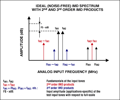
Figure 2. This plot illustrates a two-tone IMD spectrum with 2nd- and 3rd-order IMD products.
Two signal generators, containing output-leveling circuitry and linked via balanced or isolated outputs or any other coupling circuits, can easily generate IMD effects. Therefore, to avoid intermodulation distortion in the test signal, you should operate power splitters / combiners (used to combine or split two input tones) well within their linear range. Figure 3 depicts two-tone IMD with 2nd- and 3rd-order IMD products for a 10-bit, 80Msps ADC. For best results, the two-tone envelope for this ADC was chosen to be -0.5dB FS, and the amplitude for the two input tones was normalized to -6.5dB FS.
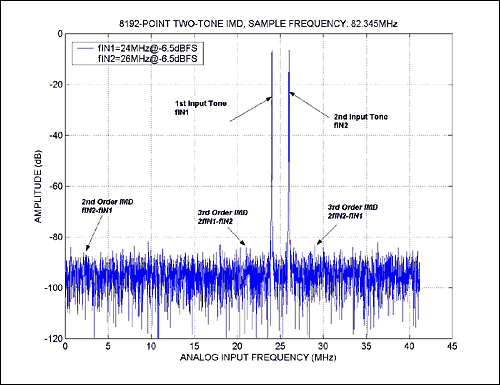
Figure 3. Two-tone intermodulation distortion for the MAX1448, with fSAMPLE = 82.345MHz.
Multi-Tone Intermodulation Distortion (Multi-Tone IMD) Multi-tone intermodulation distortion tests are often used in system design to determine limits for the signal dynamic range, useful frequency bands for different signal groups, and where to set the input signal's noise floor to mask small intermodulation components for a given ADC. The measurement of single-tone harmonic distortion is useful in obtaining general ideas about the linearity of a given ADC, but such data does not lead directly to models for predicting useful measures of intermodulation performance for independent input. -signal tones.
A typical test procedure features a computer-controlled DAC that generates a signal composed of a set of sine waves at DFT binary center frequencies. As the tone amplitudes are increased uniformly, beginning at the noise floor and continuing to the full-scale ADC level at which clipping begins, gaps between the tones serve as observation points to analyze any resulting IMD. Such tests provide results similar to that of the noise-power ratio (NPR) test (see Appendix 3). They allow better simulation of the expected signal- group waveforms, however.
Voltage Standing-Wave Ratio (VSWR) Seldom specified in the data sheets for high-speed data converters, VSWR is the ratio of mismatch between the actual impedance and the desired or expected impedance. It can be calculated by applying a test signal and measuring the reflection coefficient of the ADC input terminal. Calculated as follows, VSWR is directly related to the reflection coefficient Ï of a simple terminating impedance ZT:
VSWR = (1 + | Ï |) / (1-| Ï |),
where Ï = (ZT-Z0) / (ZT + Z0) ZT depicts the ADC input termination impedance, and Z0 represents the transmission line impedance (nominally 50Ω). To compensate for circuit inaccuracies in the measurement, it is recommended to use calibration standards if available (typically short, open, and 50Ω).
ConclusionThe preceding discussion has been a review of the most important dynamic specifications for high-speed data converters. It will conclude in Part 2, which offers detailed insight into the tools most suitable for capturing data records and for using those records in testing the dynamic performance parameters defined above. In addition to the test setup information, Part 2 provides samples of MATLAB® and LabWindows / CVI® source code, enabling designers to analyze the dynamic performance of an ADC by capturing data records quickly and processing them efficiently.
Appendices Appendix 1 The term "noise" is rather ambiguous if not qualified as to type. In general, it includes the effects of nonlinearities (INL, DNL), random and fixed-pattern effects, and sampling-time error. Total noise (ATOTAL_NOISE [ rms]) is any deviation of the output signal (converted to input units) from the input signal, excluding deviations caused by differential gain and phase errors, or DC-level shifts. Notable examples of such effects, defined here as noise, include quantization error, harmonic and intermodulation distortion, and spurious distortion.
Appendix 2 Testing high-speed ADCs for their dynamic performance often requires a frequency transform of the captured data record, using Discrete Fourier Transform (DFT) or Fast Fourier Transform (FFT) analysis. An FFT produces the same results as the DFT, but minimizes the computation requirements by taking advantage of computational symmetries and redundancies within a DFT analysis. By speeding up the computation, this approach enables a spectral analysis in virtual real time.
Provided that a periodic input signal is sampled frequently enough (ie, ≥ 2 × fMAX, where fMAX is the maximum bandwidth of the sinusoidal-input test tone, not the bandwidth of the data converter to be tested), the DFT equation pair is defined as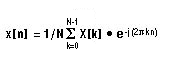
 The acquired data record usually contains sinusoidal input signals, harmonics, intermodulation products, and other spurious signals that must be analyzed to properly characterize an ADC. Assuming that all input signals are periodic, the DFT of a data record not containing an integral number of cycles of all sinusoidal input signals will contain spectral components at frequencies other than those corresponding to the chosen input tones. Also known as spectral leakage, these components should be avoided because they mask spurious performance of the ADC itself. For a precise characterization, spectral leakage must be kept at a minimum by choosing the proper input tones (with respect to fSAMPLE) and by the use of low-noise high-precision signal sources.
To avoid spectral leakage completely, the method of coherent sampling is recommended. Coherent sampling requires that the input- and clock-frequency generators are phase-locked and that you choose the input frequency based on this relationship: fIN / fSAMPLE = NWINDOW / NRECORD, where fIN is the desired input frequency,
fSAMPLE is the clock frequency of the data converter under test,
NWINDOW is the number of cycles in the data window (to make all samples unique, choose odd or prime numbers), and
NRECORD is the data record length (for an 8192-point FFT, the data record contains 8192 points).
Because the ratio of fIN and fSAMPLE is an integer value, the signal and clock sources must have adequate frequency tuning resolution to prevent spectral leakage.
Appendix 3Noise-power ratio (NPR) is a figure of merit that defines the spectral power of contributed errors, such as IMD and THD, in a small frequency band within the baseband of the composite input signal being processed and analyzed.
For this test, one generates random noise whose spectrum is approximately uniform up to a predetermined cutoff frequency less than half the sampling frequency. Then, a notch filter removes a narrow band of frequencies from the noise. To improve the measurement, the notch depth is recommended to be at least 10dB to 15dB greater than the NPR value being measured. Compared to the overall noise bandwidth, the notch width should be narrow. With this notched noise applied to the ADC input, one computes the frequency spectrum of the resulting code sequence and then calculates NPR as the ratio (in dB) of the average power spectral density inside the notched frequency band to that outside the notched band.
Literature Sources Low-Voltage / Low-Power Integrated Circuits and Systems--Low-Voltage Mixed-Signal Circuits, E. Sanchez-Sinencio & AG Andreou, IEEE Press Marketing, 1999.
MAX1448 data sheet Rev. 0, 7/00, Maxim Integrated Products.
MAX1448EVKIT data sheet Rev. 0, 7/00, Maxim Integrated Products.
Analog Integrated Circuit Design, D. Johns & K. Martin, John Wiley & Sons Inc., 1997.
Integrated Analog-to-Digital and Digital-to-Analog Converters, R. van de Plasche, Kluwer Academic Publishers, 1994.
Analog-Digital Conversion Handbook, Engineering Staff of Analog Devices Inc., PTR Prentice Hall Publishers, 1986. A similar version of this article appeared in the November 2000 issue of Microwaves and RF.
Additional Information: Dynamic Testing of High-Speed ​​ADCs, Part 2
Dynamic specifications for ADCs are very important in high-speed applications such as digital communications, ultrasound imaging, instrumentation, and IF digitization. The following discussion provides a definition and a mathematical foundation for each parameter, offers useful techniques for evaluating the dynamic performance of high -speed ADCs, and explains how the dynamic parameters correlate with ADC performance. Part 1 of this two-part discussion covers the definition of these specifications: Signal-to-noise ratio (SNR) Signal-to-noise and distortion ratio (SINAD) Effective number of bits (ENOB) Total harmonic distortion (THD) Spurious-free dynamic range (SFDR) Two-tone intermodulation distortion (TTIMD) Multi-tone intermodulation distortion (MTIMD) Voltage standing-wave ratio (VSWR) In explaining how to measure these parameters, Part 2 provides insight into the practical aspects of dynamic performance testing. Note that some specifications allow more than one approach for measure ment and even for definition. Thus, the test techniques of Part 2 represent one method and are not mandatory. Any of the methods described can be extended or altered as necessary to suit the application at hand.
When testing high-speed A / D converters, one emulates the operation of a spectrum analyzer used to quantify linearity in analog circuits. For this instrument and for the test procedure, dynamic specifications are usually expressed in the frequency domain, using the Fast Fourier Transform (FFT). In both cases, the data output represents the magnitude of this FFT. As an example (Figure 1), consider the FFT plot for an 80Msps, 10-bit ADC designed and optimized for ultrasound imaging and the digitization of baseband / IF frequencies. Such FFT plots contain impressive amounts of information and can be generated quickly. However, to make use of an FFT, one must understand how its parameters are defined.
Figure 1. 8192-point FFT plot for the MAX1448.
Signal-to-Noise Ratio (SNR) For a waveform perfectly reconstructed from digital samples, SNR is the ratio of an rms (root mean square) full-scale analog input to its rms quantization error (AQUANTIZATION [rms] = ALSB / √12 = AREF / [2N × √12]). The rms value of a sine wave is one half its peak-to-peak value divided by √2, and quantization error is the difference between an analog waveform and its digitally reconstructed replica, which is characterized by a staircase-shaped transfer curve. The difference function resembles a sawtooth wave that oscillates once per sample between the levels + 1 / 2LSB and -1 / 2LSB (LSB being least-significant bit). The difference function's rms value is its peak value (1 / 2LSB) divided by √3. For an ideal N-bit converter, SNR is defined as SNR-2N × √3 / √2 = 1.23 × 2N. Most of the dynamic specifications are expressed as a ratio of relative measurements rather than absolute units. Thus, the signal-to-noise ratio for an ideal ADC, driven by a full-sca le sinusoidal input with AC power equal to AREF / (2 × √2) in decibels, is SNRdB = 20 × log10 (AIN [rms] / AQUALITIZATION [rms]
SNRdB = 20 × log10 (AREF / [2 × √2] / AREF / [2N × √12])
SNRdB = 6.02 × N + 1.76 SNR is diminished by many noise sources in addition to quantization noise (See Appendix 1). A data converter's resolution and quantization level both help to establish its noise floor. The actual SNR for a sinusoidal input signal can therefore be described as SNRdB = 20 × log10 (ASIGNAL [rms] / ATOTAL_NOISE [rms], where ASIGNAL [rms] represents the rms amplitude for the analog input signal, and ATOTAL_NOISE [rms] is the rms sum of all noise sources (thermal noise , quantization noise, etc.) that limit the converter's dynamic performance. Applying this definition to a 10-bit ADC such as the MAX1448 yields a typical SNR value of 58.4dB at the 40MHz Nyquist frequency (fSAMPLE = 80Msps). This SNR represents 94 % of the ~ 62dB SNR exhibited by an ideal 10-bit ADC.
For an ADC driven by a sinusoidal input with an amplitude equal to the ADC's full-scale input, the maximum theoretical SNR is SNRdB = 6.02 × N + 1.76 + 10 × log10 (fSAMPLE [rms] / 2 × fMAX, where fMAX describes the maximum bandwidth of the input tone, and fSAMPLE is the converter's sampling frequency. From this equation, note that SNR increases as the sampling frequency increases beyond the Nyquist rate (2 × fMAX). Called processing gain, this effect is caused by spreading of the quantization noise power (which is fixed and independent of bandwidth) as the sampling frequency increases. This "oversampling" helps to minimize the effect of noise, which falls into the Nyquist bandwidth of DC to fMAX.
Signal-to-Noise and Distortion Ratio (SINAD) For sinusoidal input signals, SINAD is defined as the ratio of rms signal to rms noise (including the first N harmonics of THD: usually the 2nd through 5th-order harmonics). For a given sampling rate and input frequency, SINAD provides the ratio (in dB) of the analog input signal to the noise plus distortion. SINAD describes the quality of an ADC's dynamic range, expressed as the ratio of the maximum amplitude output signal to the smallest increment of output signal that the converter can produce. Mathematically, SINAD is described as SINADdB = 20 × log10 (ASIGNAL [rms] / ANOISE + HD [rms]), where ASIGNAL [rms] depicts the rms output signal level and ANOISE + HD [rms ] describes the rms sum of all spectral components below the Nyquist frequency, excluding DC. The quality of SINAD also depends on the amplitude and the frequency of a sinusoidal input tone.
Effective Number of Bits (ENOB) For actual (versus ideal) ADCs, a specification often used in place of the SNR or the SINAD is ENOB, which is a global indication of ADC accuracy at a specific input frequency and sampling rate. It is calculated from the converter's digital data record as N-log2 of the ratio of measured and ideal rms error: ENOB = N × log2 (AMEASURED_ERROR [rms] / AIDEAL_ERROR [rms]), where N is the number of digitized bits, AMEASURED_ERROR [rms] is the averaged noise, and AIDEAL_ERROR [rms] is the quantization noise error, expressed as q / √12 = AFS / [2N × √12]. AFS is the converter's full-scale input range as determined by the reference voltage AREF. ENOB = log2 (AFS / AMEASURED_ERROR [rms] × √12) or
ENOB = log2 (AREF / AMEASURED_ERROR [rms] × √12) ENOB generally depends on the amplitude and the frequency of the applied sinusoidal input tone, and both must be specified for this particular test. This method compares the rms noise produced by the ADC under test to the rms quantization noise of an ideal ADC with the same resolution in bits. If an actual 10-bit ADC with a sine-wave input of a given frequency and amplitude has an ENOB = 9.0 bits, then it produces the same rms noise level for that input as would an ideal 9-bit ADC.
Directly related to SINAD, ENOB is frequently expressed as ENOB = (SINAD-1.76) / 6.02. The error of an ideal ADC consists solely of noise. For actual converters, however, the measured error includes quantization noise along with aberrations such as missing output codes, AC / DC nonlinearity, and aperture uncertainty (jitter). Noise on the reference and power-supply lines also degrades the ENOB.
Total Harmonic Distortion (THD) Dynamic errors and integral nonlinearities contribute to harmonic distortion whenever an ADC samples a periodic signal. For pure sine-wave inputs, the output harmonic-distortion components are found at spectral values ​​whose nonaliased frequencies are integer multiples of the applied sinusoidal input tone. The amplitudes of the nonaliased frequencies, which depend on the amplitude and the frequency of the applied input sine wave, are generally given as a dB-ratio with respect to the amplitude of the applied sine-wave input. Their frequencies are usually expressed as a multiple of the frequency of the applied sinusoidal input signal.
THD is the rms sum of all harmonics in the output signal's Fast Fourier Transform (FFT) spectrum. All harmonics are included by definition, but the first three (in most cases) represent the major contribution to output distortion in a given converter. In communications and RF / IF applications, THD is often a more important figure of merit for ADCs than are the DC-nonlinearity specifications that describe the converter's static performance. THD is given by
THDdBc = 20 × log10 (√ {AHD_2 [rms] ² + AHD_3 [rms] ² + ... + AHD_N [rms] ²} / A [fIN] rms), where A [fIN] rms is the rms fundamental amplitude, and AHD_2 [rms] through AHD_N [rms] represent the rms amplitudes of the 2nd to Nth-order harmonics. The choice of harmonic components included in a set is usually a trade-off between the desire to include all harmonics with a significant portion of the harmonic-distortion energy, and the exclusion of Discrete Fourier Transform (DFT) frequency bins, whose energy content is mainly dominated by random noise (see Appendix 2).
Unless otherwise specified (refer to the manufacturer's specification in the data sheet), THD normally consists of the lowest four to nine harmonics (2nd through 10th harmonics, inclusive) of the sinusoidal analog input tone. Note that manufacturers can specify their THD values ​​either in decibels (dB) or decibels with reference to the carrier frequency or fundamental (dBc). Both units are in common use, and THD is defined with respect to the analog input tone.
Spurious-Free Dynamic Range (SFDR) The term spurious-free dynamic range is usually applied for cases in which the harmonic distortion and spurious signals are regarded as undesirable spurs in the output spectrum of a sampled pure-sinusoidal input tone. SFDR indicates the usable dynamic range of an ADC, beyond which a spectral analysis poses special detection and thresholding problems. Though similar to THD, SFDR addresses the converter's in-band harmonic characteristics.
Spurious-free dynamic range is the ratio of rms amplitude of the fundamental (the maximum signal component) to the rms value of the largest distortion component in a specified frequency range. In well-designed systems, this spur should be a harmonic of the fundamental . SFDR is important because noise and harmonics restrict a data converter's dynamic range. In an IF bandpass converter, for example, spurs can be interpreted as adjacent channel information.
In other applications, signals of interest such as low-level radar signals cannot be distinguished from the harmonic content. To help determine the SFDR value, a spectrum analyzer with an integrated digital-to-analog converter (DAC) for reconstruction is recommended. The usual procedure is to apply a near full-scale input signal (the preferred input-tone amplitude is -0.5dB to -1dB FS), measure the response, and then acquire and measure the amplitude of the largest spurious component. SFDR is the ratio of the first to the second measurement. SFDR can also be determined by inspecting the FFT spectrum (plot) of an ADC under test.
For spectrally pure sine-wave inputs, SFDR is the ratio of the amplitude of the averaged DFT value at the fundamental frequency (A [fIN]) to the amplitude of the averaged DFT value of the largest-amplitude harmonic (AHD_MAX [rms]) or spurious signal component (ASPUR_MAX [rms]) observed over the entire Nyquist band. SFDRdBc = 20 × log10 (| A [fIN] rms | / | AHD_MAX [rms] |) or SFDRdBc = 20 × log10 (| A [fIN] rms | / | ASPUR_MAX [rms] |) In general, SFDR is a function of the amplitude and the frequency (A [fIN], fIN) of the analog input tone and, in some cases, even the sampling frequency (fSAMPLE) of the converter under test. Therefore, when testing an ADC for its spurious-free dynamic range, you should specify the sampling frequency as well as the input frequency and amplitude.
Two-Tone Intermodulation Distortion (Two-Tone IMD) IMD is generally caused by modulation, and it can occur when an ADC samples a signal composed of two (or multiple) sine-wave signals. IMD spectral components can occur at both the sum ( fIMF_SUM) and the difference (fIMF_DIFF) frequencies for all possible integer multiples of the fundamental (input frequency tone) or signal-group frequencies.
For the two-tone IMD test, the input test frequencies fIN1 and fIN2 (fIN2> fIN1) are set to values ​​that are odd numbers of the DFT bins and away from the Nyquist frequencies (fSAMPLE / 2). These settings guarantee that the difference between the two input tones is always an even number of DFT bins. The resulting spectrum (Figure 2) is the averaged amplitude spectrum A [fIMF] rms. The IMD amplitudes for a two-tone input signal are found at the specified sum and difference frequencies: fIMF_SUM = | m × fIN1 + n × fIN2 | and | m × fIN1-n × fIN2 |, where m and n are positive integers. The condition that m and n are greater than zero creates the 2nd-order (fIN1 + fIN2 and fIN1-fIN2) and 3rd-order (2fIN1 + fIN2, 2fIN1-fIN2, fIN1 + 2fIN2, and fIN1-2fIN2, 3fIN1 and 3fIN2) intermodulation products.
Because test parameters are generally application-specific, no particular guidelines are necessary (or available) to specify the frequencies and signal amplitudes used for intermodulation tests. The size of | fIN2-fIN1 | depends entirely on the application and the information desired. Note that small differences in the two input tones cause the intermodulation frequencies to be clustered around the harmonic distortion components of fIN1 and fIN2.
Two-tone intermodulation distortion is generally a function of the amplitudes (A [fIN1] rms and A [fIN2] rms) and the frequencies (fIN1 and fIN2) of the input components. You must therefore specify the input tones and amplitudes for which two -tone IMD measurements are performed. It is essential that the input test signal be virtually free of intermodulation and harmonic distortion. For ADCs of larger dynamic range and wider bandwidth, this condition is increasingly difficult to achieve.
Figure 2. This plot illustrates a two-tone IMD spectrum with 2nd- and 3rd-order IMD products.
Two signal generators, containing output-leveling circuitry and linked via balanced or isolated outputs or any other coupling circuits, can easily generate IMD effects. Therefore, to avoid intermodulation distortion in the test signal, you should operate power splitters / combiners (used to combine or split two input tones) well within their linear range. Figure 3 depicts two-tone IMD with 2nd- and 3rd-order IMD products for a 10-bit, 80Msps ADC. For best results, the two-tone envelope for this ADC was chosen to be -0.5dB FS, and the amplitude for the two input tones was normalized to -6.5dB FS.
Figure 3. Two-tone intermodulation distortion for the MAX1448, with fSAMPLE = 82.345MHz.
Multi-Tone Intermodulation Distortion (Multi-Tone IMD) Multi-tone intermodulation distortion tests are often used in system design to determine limits for the signal dynamic range, useful frequency bands for different signal groups, and where to set the input signal's noise floor to mask small intermodulation components for a given ADC. The measurement of single-tone harmonic distortion is useful in obtaining general ideas about the linearity of a given ADC, but such data does not lead directly to models for predicting useful measures of intermodulation performance for independent input. -signal tones.
A typical test procedure features a computer-controlled DAC that generates a signal composed of a set of sine waves at DFT binary center frequencies. As the tone amplitudes are increased uniformly, beginning at the noise floor and continuing to the full-scale ADC level at which clipping begins, gaps between the tones serve as observation points to analyze any resulting IMD. Such tests provide results similar to that of the noise-power ratio (NPR) test (see Appendix 3). They allow better simulation of the expected signal- group waveforms, however.
Voltage Standing-Wave Ratio (VSWR) Seldom specified in the data sheets for high-speed data converters, VSWR is the ratio of mismatch between the actual impedance and the desired or expected impedance. It can be calculated by applying a test signal and measuring the reflection coefficient of the ADC input terminal. Calculated as follows, VSWR is directly related to the reflection coefficient Ï of a simple terminating impedance ZT:
VSWR = (1 + | Ï |) / (1-| Ï |),
where Ï = (ZT-Z0) / (ZT + Z0) ZT depicts the ADC input termination impedance, and Z0 represents the transmission line impedance (nominally 50Ω). To compensate for circuit inaccuracies in the measurement, it is recommended to use calibration standards if available (typically short, open, and 50Ω).
ConclusionThe preceding discussion has been a review of the most important dynamic specifications for high-speed data converters. It will conclude in Part 2, which offers detailed insight into the tools most suitable for capturing data records and for using those records in testing the dynamic performance parameters defined above. In addition to the test setup information, Part 2 provides samples of MATLAB® and LabWindows / CVI® source code, enabling designers to analyze the dynamic performance of an ADC by capturing data records quickly and processing them efficiently.
Appendices Appendix 1 The term "noise" is rather ambiguous if not qualified as to type. In general, it includes the effects of nonlinearities (INL, DNL), random and fixed-pattern effects, and sampling-time error. Total noise (ATOTAL_NOISE [ rms]) is any deviation of the output signal (converted to input units) from the input signal, excluding deviations caused by differential gain and phase errors, or DC-level shifts. Notable examples of such effects, defined here as noise, include quantization error, harmonic and intermodulation distortion, and spurious distortion.
Appendix 2 Testing high-speed ADCs for their dynamic performance often requires a frequency transform of the captured data record, using Discrete Fourier Transform (DFT) or Fast Fourier Transform (FFT) analysis. An FFT produces the same results as the DFT, but minimizes the computation requirements by taking advantage of computational symmetries and redundancies within a DFT analysis. By speeding up the computation, this approach enables a spectral analysis in virtual real time.
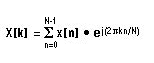
Provided that a periodic input signal is sampled frequently enough (ie, ≥ 2 × fMAX, where fMAX is the maximum bandwidth of the sinusoidal-input test tone, not the bandwidth of the data converter to be tested), the DFT equation pair is defined as
The acquired data record usually contains sinusoidal input signals, harmonics, intermodulation products, and other spurious signals that must be analyzed to properly characterize an ADC. Assuming that all input signals are periodic, the DFT of a data record not containing an integral number of cycles of all sinusoidal input signals will contain spectral components at frequencies other than those corresponding to the chosen input tones. Also known as spectral leakage, these components should be avoided because they mask spurious performance of the ADC itself. For a precise characterization, spectral leakage must be kept at a minimum by choosing the proper input tones (with respect to fSAMPLE) and by the use of low-noise high-precision signal sources. To avoid spectral leakage completely, the method of coherent sampling is recommended. Coherent sampling requires that the input- and clock-frequency generators are phase-locked and that you choose the input frequency based on this relationship: fIN / fSAMPLE = NWINDOW / NRECORD, where fIN is the desired input frequency,
fSAMPLE is the clock frequency of the data converter under test,
NWINDOW is the number of cycles in the data window (to make all samples unique, choose odd or prime numbers), and
NRECORD is the data record length (for an 8192-point FFT, the data record contains 8192 points).
Because the ratio of fIN and fSAMPLE is an integer value, the signal and clock sources must have adequate frequency tuning resolution to prevent spectral leakage.
Appendix 3Noise-power ratio (NPR) is a figure of merit that defines the spectral power of contributed errors, such as IMD and THD, in a small frequency band within the baseband of the composite input signal being processed and analyzed.
For this test, one generates random noise whose spectrum is approximately uniform up to a predetermined cutoff frequency less than half the sampling frequency. Then, a notch filter removes a narrow band of frequencies from the noise. To improve the measurement, the notch depth is recommended to be at least 10dB to 15dB greater than the NPR value being measured. Compared to the overall noise bandwidth, the notch width should be narrow. With this notched noise applied to the ADC input, one computes the frequency spectrum of the resulting code sequence and then calculates NPR as the ratio (in dB) of the average power spectral density inside the notched frequency band to that outside the notched band.
Literature Sources Low-Voltage / Low-Power Integrated Circuits and Systems--Low-Voltage Mixed-Signal Circuits, E. Sanchez-Sinencio & AG Andreou, IEEE Press Marketing, 1999.
MAX1448 data sheet Rev. 0, 7/00, Maxim Integrated Products.
MAX1448EVKIT data sheet Rev. 0, 7/00, Maxim Integrated Products.
Analog Integrated Circuit Design, D. Johns & K. Martin, John Wiley & Sons Inc., 1997.
Integrated Analog-to-Digital and Digital-to-Analog Converters, R. van de Plasche, Kluwer Academic Publishers, 1994.
Analog-Digital Conversion Handbook, Engineering Staff of Analog Devices Inc., PTR Prentice Hall Publishers, 1986. A similar version of this article appeared in the November 2000 issue of Microwaves and RF.
LabWindows is a registered trademark of National Instruments Corporation.
MATLAB is a registered trademark of The MathWorks, Inc.
Ebike Battery,Electric Scooter Battery,48V Electric Bike Battery,Batteries For Electric Bike
Zhijiang BSL battery technology service company , https://www.bslbatteryservice.com