Abstract: Introduce the real-time digital image wireless transmission system based on the WE904 wireless transceiver module, and the interface circuit hardware design of the system. Discuss the problem of bit error caused by low frequency components in FSK input signal and its solution.
introduction
With the maturity of short-range, low-power wireless data transmission technology, especially the promotion of Bluetooth, 802.11b and other applications, wireless data transmission applications have once again become a hot spot for applications. This article introduces a wireless transceiver module based on Singapore Winedge's WE904 chip, and illustrates its application in a real-time wireless image data transmission system to achieve a low transmission power and low cost practical application system. Provide a new solution for low-cost, low-speed wireless data transmission.
1 System Introduction
The simple block diagram of the system is shown in Figure 1. The simple working process of this system is: ①The computer eye is responsible for image acquisition and A / D conversion of image signals. ②The image signal output by the computer eye is encoded and compressed by the DSP chip TMS320VC5402 (hereinafter referred to as 5402). ③5402 realizes the interface with WE904 module through McBSP (multi-channel buffer serial port), realizes the configuration of WE904 module, and outputs the encoded image signal to WE904 module in RS232 protocol signal format, and sends it out after modulation. ④ The WE904 module at the receiving end outputs a TTL level signal, and after the level conversion of the RS232 level interface, the serial port is input to the PC. ⑤ The PC decodes and displays the received image signal.
2 Introduction of WE904 wireless transceiver module WE915CTX1
The main chip of WE915CTX1 wireless transceiver module is WE904 of Singapore Winedge company. 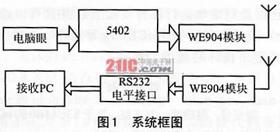 WE904 is a single-chip FM transceiver chip that supports full-duplex. Only a few external components are needed to implement wireless transceiver functions. The operating frequency range can be from 0.1GHz to 1GHz. WE904 provides a serial programming interface. Through the serial programming interface, you can flexibly adjust the transceiver frequency, signal output mode, whether to support full-duplex and other parameters. This system directly used the module WE915CTX1 of WE904 in the early stage of design. WE915CTX1 integrates the WE904 chip and required external components, and provides a concise interface for use, which can be easily embedded into the application system. Its main features are:
①Work in 902MHz ~ 928MHz American ISM frequency band, can provide 20 channels;
â‘¡Using FM / FSK modulation mode, the channel width is 100kHz;
â‘¢ Provide two output modes of digital signal and analog signal, which can be used for the transmission of digital and analog signals;
â‘£ Sensitivity is -115dBm;
⑤When the low output power is 0dBm, it can provide about 80m (digital signal) and 300m (voice and other analog signals) effective transmission distance
â‘¥The transmission rate can reach 57.6kbps, which is related to the transmission distance;
⑦Provide serial programming interface, may flexibly configure the parameters such as transceiver frequency;
⑧ Provide RSSI received signal strength indication.
3 WE904 module WE915CTX1 interface
WE915CTX1 provides a simple user interface, as shown in Figure 2. ①VCC and GND are power supplies, and the power supply voltage is 3.3 to 4.5V. ② Audio In is the input pin of the baseband signal to be modulated. The input signal can be an analog signal such as voice or a digital signal. The requirement for the input signal is that its AC effective value is usually 140mV ~ 200mV, a larger input effective value can get a better signal-to-noise ratio, but will also occupy a larger bandwidth. Usually 200mV will produce a frequency deviation of 25kHz. When a digital signal with a TTL level is input to the Audio In pin, the effective value of its voltage must be reduced first. This can be achieved by using two series resistors to divide the voltage. For example, you can use a 10kΩ and a 1.8kΩ resistor in series to divide the voltage, but the resistance of the resistor used should not be too large, otherwise the input square wave waveform will be seriously distorted. ③ Audio Out is the output pin of the received signal. When the output mode is set to analog output (analog), the effective value of the output signal is usually 140mV ~ 180mV of the demodulated baseband signal. When the output mode is set to digital mode (digital), the output signal Vp-p is a digital signal square wave of about 3V. ④LNA_ON is the power control pin of low cry amplifier, low level is effective. It must be set low during reception to obtain a gain of about 15dB; it can be turned off when no signal is received to reduce power consumption. ⑤ANT is the antenna connection pin, and its output impedance is 50Ω. ⑥ RSSI is a reminder of received signal strength. When the received signal changes from -110dBm to -50dBm, the RSSI level changes from 0.65V to 1.70V. ⑦CLK, DATA and LE are serial programming control ports, used to realize programming control of WE904 chip. It will be described in detail below. 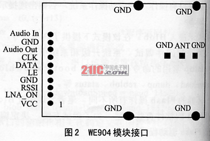
4 WE904 module WE915CTX1 programming control interface
There are 4 control registers inside WE904 chip, used to control the working state of WE904 chip. The four registers are the reference frequency register, transmit frequency register, receive frequency register and mode register. The function definition of the corresponding bits of these 4 control registers is not introduced here, the reader can refer to the chip information of W904. The write control of these four registers is realized through the three pin industries of CLOCK, DATA and LE, which correspond to the CLK, DATA and LE of the analog WE915CTX1 respectively. The write timing is shown in Figure 3.
The basic process of writing is: ①Low level at the beginning of LE. ②When LE becomes high level, the data starts to move into the internal shift register from the DATA pin under the drive of CLOCK. The data shift operation is performed on the rising edge of CLOCK. Therefore, when designing the interface, the falling edge of the clock CLOCK is usually aligned with the bit boundary, so that the data can be effectively sampled on the rising edge of CLOCK. ③ After the last data is shifted into the internal shift register, LE goes low before the next clock rising edge. On the falling edge of LE, data will be written into the control register by the internal shift register. ④ Which one of the four control registers the data is written to is determined by the value of the lowest two bits of DATA. These two bits are called load control bits. ⑤WE915CTX1 requires that the data of DATA has been kept at least 45ns before the rising edge of CLOCK, so the frequency of CLOCK should not be too high.
5 5402r McBSP Introduction
5402 is a general purpose DSP chip with excellent cost performance of TI company, which has a wide range of applications. It provides two McBSPs. McBSP is a full-duplex high-speed synchronous serial port that can be used for high-speed serial communication with other DSP chips and codecs in the system. The operation of McBSP is controlled by a series of registers in the DSP chip. Fig. 4 is the standard operation sequence of McBSP. Whether it is a shift operation of transmission or reception, are triggered by the rising edge of the frame synchronization signal FSX or FSR, and by the clock CLKR or CLKX to synchronize the bit boundary. There can be a delay of several clocks from the rising edge of FSX or FSR to the beginning of the shift operation. Figure 4 shows the delay of 1 clock. This can be set by the corresponding bits in the control registers XCR2 and RCR2. The number of bits of data sent or received after each frame synchronization signal is also set in the control registers XCR2 and RCR2. Figure 4 is the simplest operation sequence of McBSP, which is sufficient for general applications and more powerful. Functionality requires a more complex design. 
6 Interface design of 5402 and WE904 module
In the design of this system, the sending of image data and the programming configuration of the WE904 module are done using the same McBSP of the DSP chip 5402. This makes the two processes independent of each other, and an I / O pin XF of 5402 is also used in the design. Figure 5 shows the simple principle of the interface circuit. The basic principles are as follows: ①During the configuration of the WE904 module, XF is high, the input of LE is determined by McBSP's transmission frame synchronization FSX, and the transmission clock CLKX and transmission data line DX are driven CLK and DATA of WE904 module. ②In order to configure the WE904 module, the setting of McBSP is FSX cycle greater than 24 CLKX clock cycles, and the high level width is set to 24 CLKX clock cycles. CLKX first inverts when driving CLK. In this way, you can get roughly the same timing as Figure 4, and you can complete the configuration of the WE904 module. Here are the reference values ​​of McBSP control registers: SPCR1 = 0x0080, SPCR2 = 0x0262, RCR1 = 0x0000, SRGR2 = 0x301f, MCR1 = 0x0000, MCR2 = 0x0000, PCR = 0x0b02. ③ After the configuration of the WE904 module is completed, XF is set to low level output, at this time the input value of LE is always high level, therefore, the input of CLK and DATA will not change the setting of WE904. At this time, the transmitted image data is serially output from the DX and input to the Audio In of the EW904 module after being divided. The transmitted clock CLKX is input from the FSR pin. This is mainly because the DSP clock of this system is 100MHz. After the DSP clock is divided by the internal counter, the required tens of kHz clock cannot be obtained from the CLKX pin. The required clock must be divided again (in the register FPER Set the frequency division parameter in F), and get it from FSG, and the sending frame synchronization FSX will be set to be automatically generated when the data is copied from DXR to XSR. During the configuration of the module, FSR is set as an input and does not affect the input value of CLK. ④XF undergoes an inversion before doing OR operation with FSX, mainly because XF is also used for the control of other structures in this system. During the transmission of the image, XF is required to be low.
Figure 4
7 RS232 asynchronous serial communication
This system uses RS232 asynchronous serial communication protocol. The RS232 asynchronous serial communication interface is a traditional peripheral interface of a microcomputer. It is characterized by simple use, but the rate is low. The RS232 interface has a wide range of applications in low-speed data transmission, industrial control, and industrial data collection. Because the image data to be transmitted by this system has been well compressed, the rate is in the tens of kbps, so this system uses RS232 serial port for communication. When handshake is not required, the simplest serial communication requires only 3 lines to complete the connection, and unidirectional communication even requires only 2 lines. However, because the level of the RS232 serial interface is higher (usually plus or minus 4V ~ 12V), which is different from the usual TTL level, it must undergo the necessary level conversion. This system uses MAXIM MAX232 to complete level conversion. The data format of the RS232 communication protocol is shown in Figure 6. During the transmission of each byte, it starts with a start bit and ends with a stop bit (the number of stop bits can be set). The parity bit can be added before the stop bit, and idle bits can also be inserted between each byte. The start bit is 0 and the stop bit is 1. The idle bit is also 1, which has the same level as the stop bit. The receiving serial bus starts to receive data when it detects the falling edge of the start bit. In this system design, since the data is transmitted in one direction, the data format of RS232 is directly constructed by McBSP. Then sent to the WE904 module's Audio In modulation and sent. If two-way data transmission is required, an asynchronous serial communication interface chip can be added, such as TI's TL16C750. The receiver's microcomputer is responsible for serial data reception. There are usually three kinds of writing of serial port receiving programs: â‘ Use C or assembly language to control the hardware; â‘¡ Use Windows API functions; â‘¢ Use Mscomm control provided by VB. This system uses VB's Mscomm control. This method is relatively simple, but the efficiency is slightly lower, if you need a more efficient program, you can choose the first two methods. There is a lot of information about the serial port transceiver program, which will not be detailed here. 
8 Bit errors caused by low frequency components in FSK wireless data transmission
In FSK wireless data transmission, low frequency components in the input signal may cause a high bit error rate. The specific performance in the two-phase FSK is that when the number of "1" or "0" in the input signal increases significantly within a short period of time, the bit error rate of the received signal also increases significantly. This is mainly because the entire system divides the low frequency in the signal into attenuation, such as the effect of the DC blocking coupling capacitor in the system. After the low-frequency component is attenuated, the signal cannot be recovered correctly, which causes a high bit error rate. To improve system performance, the low-frequency components in the input signal must be kept as small as possible and kept constant. This is called the equalization problem. For a simple binary input, it is necessary to make the number of 1s and 0s in the input signal as balanced as possible. Generally, in order to reduce low-frequency components, the input signal can be HDB3 encoded and Manchester encoded. HDB3 is a ternary input code. There are three levels in signal transmission, which need to be realized by special hardware. Manchester codes are binary codes. Its simple rules are: 1 is represented by a transition from 1 to 0, and 0 is represented by a transition from 0 to 1. Obviously after using Manchester encoding, the number of 1 and 0 reached a complete balance, but at the same time it doubled the amount of data. Considering the requirement of data volume, this system borrows the 5B6B code used in high-speed optical fiber communication in the design. 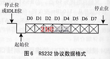 5B6B coding expresses 5-bit binary numbers with 6-bit binary numbers. It selects 32 groups from 64 combinations of 6-bit binary numbers to encode the signal codes. There are two kinds of positive mode and negative mode when coding. When used, it is selected in pairs to make the number of 1, 0 codes in the code sequence tend to balance. 5B6B has the characteristic that the maximum number of consecutive links in the transmission sequence is five. The accumulated difference of 1, 0 codes (called digital sum) varies within the range of -3 to +3. The 5B6B code solves the problem of equalization of 1 and 0 in the input signal, and has higher transmission efficiency. It only increases the number of codes by 20%. After this system adopts 5B6B coding (before RS232 output), it has achieved a very obvious effect in reducing the bit error rate of the system.
Conclusion
This system uses the WE904 module for real-time wireless digital image transmission experiments. It uses a common single antenna. When the transmission rate is 57.6kbps and the extremely low transmission power is 0dBm, the visible transmission distance is greater than 100m. ). Using its own image compression algorithm, it can stably transmit 3 to 6 frames of images per second (384 & TImes; 288 pixels for black and white images). It provides a very competitive reference solution for low-cost, medium- and low-speed wireless data transmission.
Ipa Snap Swab For Atm Cleaning,Snap Swab For Atm Cleaning,Swab For Atm Cleaning,Ipa Swab For Atm Cleaning
Miraclean Technology Co., Ltd. , https://www.mrccleanroom.com