Abstract: nRF24E1 is a highly integrated wireless transceiver chip that integrates 2.4GHz wireless transceiver, enhanced 8051, ADC and other peripherals. It has small size, low power consumption, few peripheral components, and has a large The price advantage can replace the Bluetooth application requirements in some occasions. The main features, internal structure and pin functions of the nRF24E1 chip are introduced in the article, and finally the wireless data packet format and typical application circuit of nRF24E1 are given.
1 Main features of nRF24E1
nRF24E1 is a wireless transceiver module launched by Nordic Integrated Circuit Corporation (NORDIC) with 2.4GHz wireless transceiver nRF2401 and enhanced 8051 core. nRF24E1 is suitable for short-distance interconnection applications of various wireless devices, and works in the ISM (Industrial, Scientific and Medical) frequency band. The device has 125 frequency points, can achieve point-to-point, point-to-multipoint wireless communication, and can use frequency change and frequency hopping to avoid interference. The maximum transmission rate of nRF24E1 is up to 1 Mbit / s, and its maximum transmission power is 0 dBm. In a more ideal environment, its indoor transmission distance can reach 30 to 40 meters, and outdoor transmission distance can reach 100 to 200 meters. The sensitivity of nRF24E1 is -90dB, the working voltage is 1.9V ~ 3.3V, and the working temperature range is -40 ~ + 80 ℃.
The main features of nRF24E1 are as follows:
â— With 2.4GHz wireless transceiver; 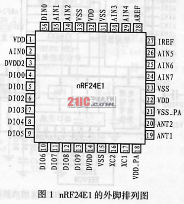
â— Contains enhanced 8051 controller;
â— Can work under low voltage? 1.9V ~ 3.6V ?;
â— There is a voltage regulator inside;
◠Standby current can be as low as 2μA, and the device also has a wake-up timer;
◠Manufactured with CMOS technology of 0.18μm;
â— Very few peripheral devices required;
â— Simple design.
2 Pin function
nRF24E1 is packaged in 36-pin QFN (6 & TImes; 6mm), and its pin arrangement is shown in Figure 1. The functions of each pin are as follows:
nRF24E1 has 11 digital I / O pins, which are composed of P0 port (DIO2 ~ DIO9) and P1 port (DIO0, DIO1, DINO0). Except that DINO0 can only be used for input, the rest are bidirectional pins, and most of them Digital I / O has multiplexing function. The multiplexing function of each pin of P0 port is listed in Table 1.
Table 1 Multiplexing function of P0 port pins
| Lead | P0.7 (DIO9) | P0.6 | P0.5 | P0.4 |
| Reuse function | PWM | T1 | T0 | INT1 |
| Lead | P0.3 | P0.2 | P0.1 | P0.0 (DIO2) |
| Reuse function | INT0 | TXD | RXD | GPIO |
In addition, P0 port has two control registers P0 ALT and P0 DIR. Among them, the control priority of P0 ALT is higher than that of P0 DIR. During design, you can set P0 ALT to determine which pins use multiplexing function. Pins without multiplexing function are GPIO, and you can use P0 DIR to set whether these P0 ports are input or output.
P1 port has only 3 pins, which can be set as SPI interface or GPIO. When nRF24E1 uses SPI, it can only be used as a host. The pin functions of the SPI interface are as follows:
P1.2 (DIN0): serial data input pin;
P1.1 (DIN1): serial data output pin;
P1.0 (DIO0): Serial clock pin.
nRF24E1 has 9 analog input pins, among which AIN0 ~ AIN7 are 8 analog inputs of ADC, and AREF is ADC reference voltage. In addition, the device has two antenna interface pins ANT1 and ANT2 and two crystal pins XC1 and XC2.
nRF24E1 must use high-precision crystal oscillator, in order to support the transmission rate of 1Mbit / s, the design must also use more than 16MHz crystal oscillator.
There are 12 other pins of nRF24E1. IREF is used to connect an external bias reference resistor. The rest are power and ground pins.
figure 2
3 Internal structure
Figure 2 is the internal structure block diagram and peripheral components of nRF24E1.
As can be seen from the internal structure of the chip, nRF24E1 has an enhanced 8051 core, a wireless transceiver nRF2401, a 9-bit 100kbps / s 10-bit analog-to-digital converter, a UART asynchronous serial port, a SPI interface, a PWM output, an RC oscillator. Watchdog and wake-up timer, in addition, nRF24E1 also built a special voltage regulator circuit.
In the internal storage space of nRF24E1, 512B ROM is used to store the boot program. After power on, it can download the program stored in EEPROM to the program running space of 4KB RAM, and the other 256B RAM is data storage.
4 Wireless data packet format and transceiver configuration word
The data packet format is an important part of the communication protocol. The wireless data packet format of nRF24E1 is as follows:
| Peramble | ADDR | PAYLOAD | CRC |
Among them, Prameble is the preamble, which is automatically added by the hardware; ADDR is the 32- to 40-bit address code to be sent; PAYLOAD is valid data; CRC is the CRC checksum, which can be automatically added by the built-in CRC error correction hardware circuit Up, can be set to 0, 8 or 16 digits. The total length of ADDR, PAYLOD, and CRC is a maximum of 256 bits. Therefore, setting a shorter address and checksum can improve transmission efficiency, but will reduce reliability.
The wireless transceiver nRF2401 has a 144bit configuration word that specifies the wireless transceiver's receive address, transceiver frequency, transmit power, wireless transmission rate, wireless transceiver mode, and the length of the CRC checksum and the length of the valid data. At the same time, the wireless transceiver can only be in one of the receiving or transmitting modes, generally the receiving mode is the standby state.
5 Application circuit
nRF24E1 can work in the 2.4GHz international general-purpose ISM band without applying for a wireless application license, which greatly facilitates developers and users. nRF24E1 built-in enhanced 8051 controller, is a set of wireless data reception and transmission in one? and can process data on-chip system (SOC), which makes the application system of nRF24E1 more simplified, and greatly enhance the wireless system The stability and reliability of the software also make development simple and reduce costs.
image 3
nRF24E1 is small in size and low in power consumption, so it is very suitable for applications requiring high volume and power consumption. It can be widely used in computer peripherals, wireless headphones, toys, gamepads, automotive electronics, medical equipment, remote control and industrial sensors. Figure 3 shows the application circuit of nRF24E1. In the picture, nRF24E1 is connected to EEPROM through the SPI port. After power on, the circuit can transfer the user program stored in EEPROM to the 4KB RAM program running space of nRF24E1 under the control of the boot program stored in 512B ROM to transfer the control task to the user program. You can communicate with other devices through the SPI port.
After power-on, you must first initialize the configuration word of the wireless transceiver nRF2401, which can be achieved by writing data to the configuration word in 8051.
6 Conclusion
As we all know, Bluetooth chips also work in the 2.4 GHz frequency band, but due to their high cost, products are difficult to develop, so? So far, there are few Bluetooth market products. In addition, the market also has no application requirements that require Bluetooth. In this way, some of Bluetooth's market positioning can be easily replaced by other more professional products. NRF24E1 is one of which has a price advantage and is easier to develop. Available To replace the needs of Bluetooth applications in some areas
Measurement data can be sent via PufangTech`s RS485 Wireless Modem for point to point or point to multi-point data communication with a range of 1km to 50km. It provides a transparent half duplex radio serial connection wirelessly operating in VHF/UHF frequency band.
The parameters of the wireless modems can be configured through the local serial port using Windows based software. The individual configuration parameters can be stored on PC for future use.
PufangTech wireless modem equipped with LEDs which enable the operator to see at a glance the status of the modem and its interfaces. The LEDs provide the operator with a quick visual check and if the modem is in normal operation, configuration or alarm status.
RS485 Wireless Modem is developed for remote supervision and control applications. Typical target applications such as slave stations of oil, gas and water pipelines, environmental monitoring, street light control, wastewater pumping stations and OEM applications.
RS485 Wireless Modem
RS485 Wireless Modem,RS485 Wireless Data Radio Modem,RS485 Wireless GSM Modem,RS485 Wireless Router Modem
Shenzhen PuFang Technology Co., Ltd. , https://www.hytelus.com