In the communications infrastructure, the rise of femtocells and picocells is driving the base station toward smaller miniaturization, which imposes complex requirements on the power supply of digital baseband, memory, RF transceivers and power amplifiers, and must be provided in a minimum area. The highest power density is shown in Figure 1. A typical small cell system requires a very dense power supply that delivers large currents in fast transient response to power the digital baseband while utilizing a low noise, low dropout regulator (LDO) for the AD9361 RF agile transceiverTM, temperature compensated The crystal oscillator (TCXO) and other noise-critical power rails are powered. Setting the switching regulator's switching frequency outside of the critical RF band reduces noise, and the synchronous switching regulator ensures that the beat frequency does not affect RF performance. Lowering the digital baseband core voltage (VCORE) minimizes power consumption in low-power modes, and power sequencing controls ensure that the digital baseband powers up and operates before the RF transceiver is enabled. The I2C interface between the digital baseband and power management allows the output voltage of the buck regulator to be changed. To improve reliability, the power management system can monitor its own input voltage and die temperature to report any faults to the baseband processor.
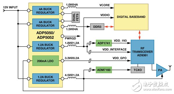
Figure 1. Small base stations require multiple power supplies
Similarly, the trend in medical and instrumentation (such as portable ultrasound devices and handheld instruments) is also getting smaller and smaller, requiring a more efficient way to power FPGAs, processors, and memories in a much smaller area, as shown in Figure 2. Show. Typical FPGA and memory designs require a very dense power supply that can deliver large currents with fast transient response to power the core and I/O supply rails while on-chip analog to a phase-locked loop (PLL) through a low-noise rail. Circuit power supply. Power sequencing is critical and should ensure that the FPGA powers up and runs before the memory is enabled. Regulators with precision enable inputs and dedicated power good outputs support power sequencing and fault monitoring. Power designers often want to use the same power IC in different applications, so the current limit must be changed. This design reuse can dramatically reduce time-to-market – one of the key elements in any new product development process.
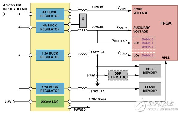
Figure 2. Powering an FPGA-based system
Consider common design specifications for multi-rail power management for FPGAs with 1 12 V input and 5 outputs:
Core rail: 1.2 V (4 A)
Auxiliary track: 1.8 V (4 A)
I/O rail: 3.3 V (1.2 A)
DDR memory rail: 1.5 V (1.2 A)
Clock rail: 1.0 V (200 mA)
A typical discrete scheme is shown in Figure 3a, with four switching regulators connected to the 12 V input rail. The output of a switching regulator pre-conditioning the LDO to reduce power consumption. Another method, shown in Figure 3b, uses a voltage regulator to step down the 12 V input to a 5 V intermediate rail and then adjust to produce the desired voltage. The cost of this solution is lower, but the efficiency is also lower due to the two-stage power conversion. In both options, each regulator must be independently enabled, so a dedicated power sequencing controller may be required to control the timing of the power supply. Noise can also be a problem unless all switching regulators can be synchronized to reduce the beat frequency.
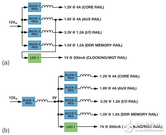
Figure 3. (a) Discrete voltage regulator design, (b) Alternative discrete voltage regulator design
Integrated solution for high efficiency, small size
Integrating multiple buck regulators and LDOs into a single package significantly reduces the overall size of the power management design. In addition, intelligent integrated solutions offer many advantages over traditional discrete solutions. Reducing the number of discrete components can significantly reduce the cost, complexity, and manufacturing cost of the design. The integrated power management unit (PMU) ADP5050 and ADP5052 enable all of these voltages and functions in a single IC, resulting in a significant reduction in PCB area and components.
To maximize efficiency, the pre-regulator stage is removed and each buck regulator is powered directly from the 12 V voltage (similar to Figure 3a). Buck regulators 1 and 2 have programmable current limits (4 A, 2.5 A, or 1.2 A), so power supply designers can quickly and easily change current for new designs, dramatically reducing development time. The LDO can be powered from a 1.7 V to 5.5 V supply. In this example, the 1.8 V output of one of the buck regulators powers the LDO and provides a low noise 1 V supply rail for noise sensitive analog circuitry.
The switching frequency fSW is set by the resistor RRT and ranges from 250 kHz to 1.4 MHz. The flexible switching frequency range allows the power supply designer to optimize the design, reduce the frequency for maximum efficiency, or increase the frequency to achieve the smallest overall size. Figure 4 shows the relationship between fSW and RRT. The value of RRT can be calculated by:
RRT = (14822/fSW) 1.081, the unit of R is kΩ, and the unit of f is kHz.
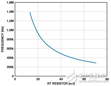
Figure 4. Switching frequency vs. RRT
In some designs, both are important: lower switching frequencies are used for higher current rails to provide maximum power efficiency, and higher switching frequencies are used for lower current rails to reduce inductor size and achieve minimum PCB area. The ADP5050's main switching frequency has a divide-by-2 option that can operate at two frequencies, as shown in Figure 5. The switching frequency of buck regulators 1 and 3 can be set to half of the main switching frequency through the I2C port.
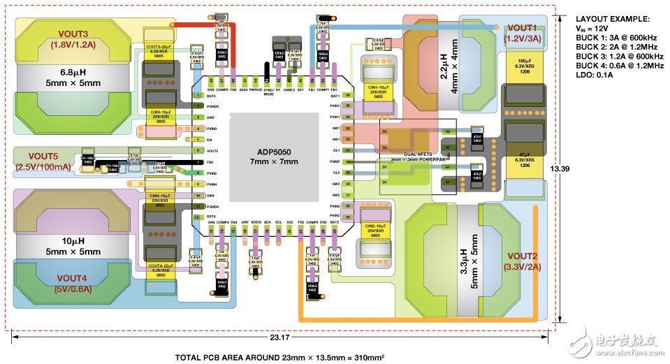
Figure 5. ADP5050 uses low switching frequency for high current rails to increase efficiency and high switching frequency for low current rails to reduce inductor size
Power sequencing
As shown in Figure 6, the ADP5050 and ADP5052 simplify power supply timing control for applications using FPGAs and processors through four features: precision enable inputs, programmable soft-starts, power good outputs, and active output discharge switches.
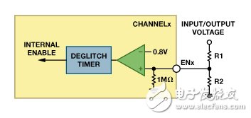
Precision Enable Input: Each regulator, including the LDO, has an enable input with a precision reference of 0.8 V (Figure 6-1). The regulator is enabled when the enable input voltage is greater than 0.8 V; the regulator is disabled when the voltage is less than 0.725 V. An internal 1 MΩ pull-down resistor prevents an error from occurring when the pin is left floating. With the precision enable threshold voltage, it is easy to control the power supply timing within the device, as is the case with an external power supply. For example, when buck regulator 1 is set to 5 V, a resistor divider can be used to set the exact 4.0 V trip point to enable buck regulator 2, and so on to set precise power-up timing for all outputs. .
Programmable soft start: The soft start circuit slowly increases the output voltage in a controlled manner to limit the inrush current. When the soft-start pin is connected to VREG, the soft-start time is set to 2 ms; when a resistor divider is connected between the soft-start pin and VREG and ground, the soft-start time can be increased to 8 ms (Figure 6-2) . This configuration may be required to support a specific boot sequence or a value with a large output capacitance. The soft-start configurability and flexibility enable large, complex FPGAs and processors to power up in a safe and controllable manner.

1. The precision enable threshold is above 0.8V to enable the regulator, and below 0.72V (hysteresis) the regulator is turned off. 2. Programmable soft start The different soft start on each channel can be programmed to be 2ms, 4ms, 8ms.

3. The required PWRGDx for PWRGD output CH1 to CH4 can be configured via factory fuse or I2C. 4. The active output discharge switch can turn on the output discharge switch to shorten the discharge period of the output capacitor.
Figure 6. ADP5050 and ADP5052 Simplified Power Supply Timing Control
Power Good Output : When the selected buck regulator is operating normally, the open drain power good output (PWRGD) goes high (Figure 6-3). A good power pin informs the host system of the condition of the power supply. By default, PWRGD monitors the output voltage on buck regulator 1, but other channels can be customized to control the PWRGD pin. The status of each channel (PWRGx bit) can be read back via the I2C interface on the ADP5050. A logic high on the PWRGx bit indicates that the regulated output voltage is above 90.5% of the nominal output. When the regulated output voltage drops below 87.2% of its nominal output for more than 50 μs, the PWRGx bit is set to logic low. The PWRGD output is the logical sum of the internal unshielded PWRGx signals. The internal PWRGx signal must be high for at least 1 ms for the PWRGD pin to go high; if any PWRGx signal fails, the PWRGD pin goes low without delay. The channel that controls PWRGD (channel 1 to channel 4) is specified by the factory fuse or by the corresponding bit set by the I2C interface.
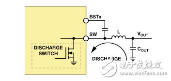
Active Output Discharge Switch : Each buck regulator incorporates a discharge switch that is connected between the switch node and ground (Figure 6-4). When its associated regulator is disabled, the switch is turned on, helping to quickly discharge the output capacitor. For Channel 1 to Channel 4, the typical resistance of the discharge switch is 250 Ω. When the regulator is disabled, the active discharge switch pulls the output to ground even with large capacitive loads. This can significantly improve the stability of the system, especially during cycle power.
Figure 7 shows a typical power-up/power-down sequence.
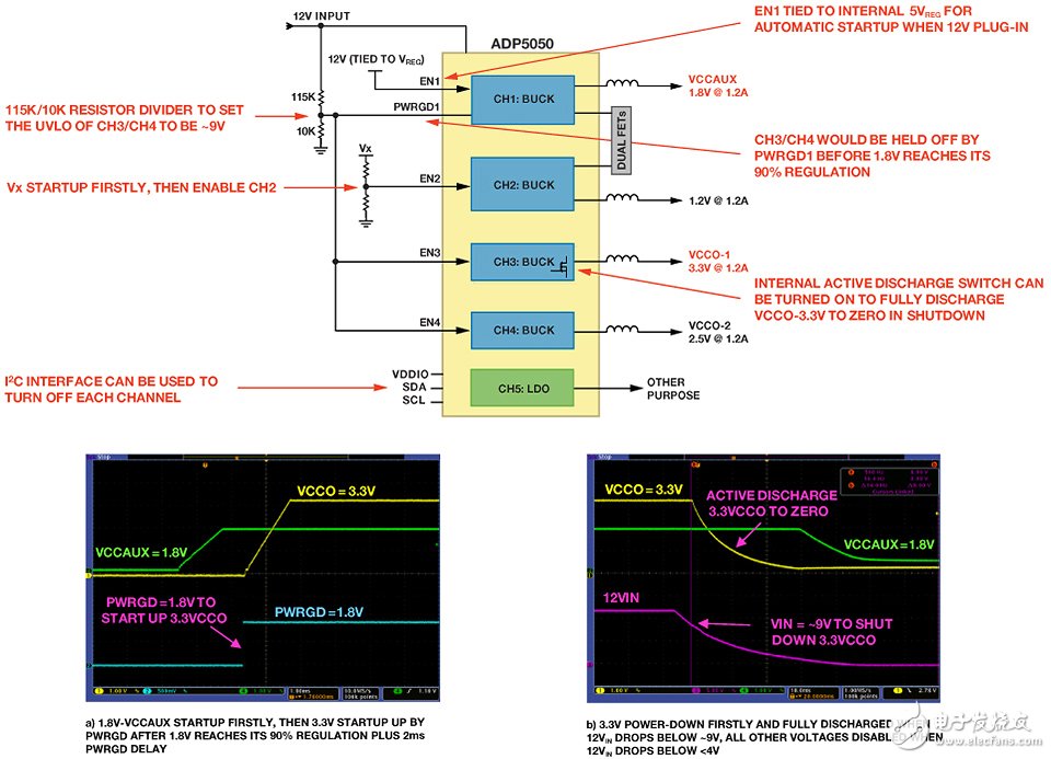
Figure 7. Typical Power-Up/Shutdown Timing
I2C interface
The I2C interface enables advanced monitoring and basic dynamic voltage scaling of the two buck regulator outputs (Channel 1 and Channel 4).
Input voltage monitoring : It can monitor the input voltage for faults such as undervoltage. For example, applying a 12 V voltage to the input, the I2C interface is configured to trigger an alarm if the input voltage is below 10.2 V. A signal on the dedicated pin (nINT) tells the system that a processor problem has occurred and shuts down the system to take corrective action. The ability to monitor input voltage increases system reliability. Figure 8 shows which values ​​can be set to monitor the input voltage of the ADP5050.
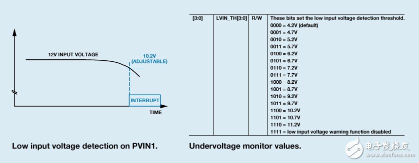
Figure 8. Input undervoltage detection
Junction temperature monitoring : The junction temperature can be monitored to determine if an overtemperature fault has occurred. If the junction temperature is higher than the preset value (105 ° C, 115 ° C or 125 ° C), an alarm signal will be generated on nINT. Unlike thermal shutdown, this feature sends a warning signal without shutting down the device. The ability to monitor the junction temperature and alert the system processor to avoid system failures can improve system reliability, as shown in Figure 9.
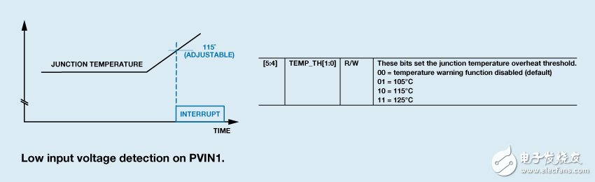
Figure 9. Junction temperature monitoring
Dynamic Voltage Regulation : Dynamic voltage regulation reduces system power by dynamically reducing the supply voltage of Channel 1 and Channel 4 in low-power mode. It can also dynamically change the output voltage based on system configuration and load. In addition, the output voltages of all four buck regulators can be set through the I2C interface, as shown in Figure 10.
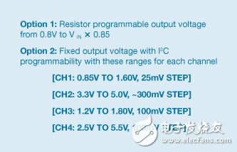
Figure 10. ADP5050 Output Voltage Options
Low noise characteristics
Multiple features reduce system noise generated by the power supply.
Wide Resistor Programmable Switching Frequency Range: The resistor on the RT pin sets the switching frequency from 250 kHz to 1.4 MHz. The power designer has the flexibility to set the switching frequency to avoid system noise bands.
Buck Regulator Phase Shift: The phase shift of the buck regulator can be set via the I2C interface. By default, the phase shift between channel 1 and channel 2 and between channel 3 and channel 4 is 180°, as shown in Figure 11. The advantage of inverting operation is lower input ripple current and power supply ground noise.
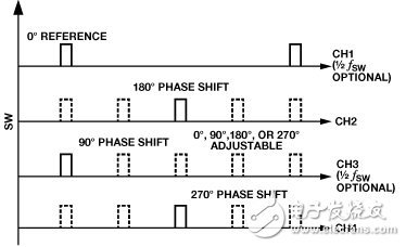
Figure 11. Buck Phase Regulator Phase Shift for the ADP5050/ADP5052
Figure 12. Phase shift of the buck regulator can be configured through the I2C interface
Clock Synchronization : The switching frequency can be synchronized to an external clock from 250 kHz to 1.4 MHz via the SYNC/MODE pin. This capability is important for RF and noise sensitive applications. When an external clock is detected, the switching frequency smoothly transitions to its frequency. When the external clock is stopped, the device switches to the internal clock and continues to operate normally. Synchronization with an external clock keeps the system designer away from the critical noise band and reduces the noise generated by multiple devices in the system.
For successful synchronization, the internal switching frequency must be set to a value close to the external clock value, and the frequency difference is recommended to be less than ±15%.
The SYNC/MODE pin can be configured as a synchronous clock output via a factory fuse or I2C interface. When the frequency is equal to the internal switching frequency, the SYNC/MODE pin generates a positive clock pulse with a 50% duty cycle. There is a short delay time (about 15% of the tSW) between the generated synchronous clock and the channel 1 switch node.
Figure 13 shows two devices configured in frequency-synchronous mode: one device is configured as a clock output to synchronize another device. A 100 kΩ pull-up resistor should be used to prevent a logic error when the SYNC/MODE pin is left floating.
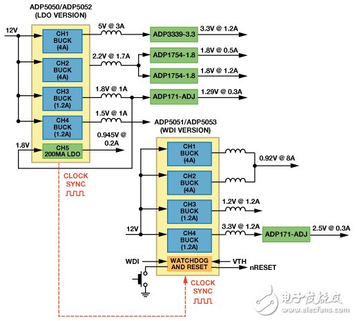
Figure 13. RF application shows two devices synchronized to reduce power supply noise
Both devices are synchronized to the same clock, so the phase shift between channel 1 of the first device and channel 1 of the second device is 0°, as shown in Figure 14.
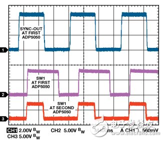
Figure 14. Waveforms of two ADP5050 devices operating in synchronous mode
ADIsimPower design tool
ADIsimPowerTM now supports multi-channel high-voltage PMUs ADP5050/ADP5052, which supply up to 4/5 channels from inputs up to 15 V with load currents up to 4 A per channel. With this design tool, the user can cascade the channels and place the high current channels in parallel to form an 8 A power rail, taking into account the heat distribution of each channel to optimize the design. With advanced features, the user can independently specify the ripple and transient performance of each channel, the switching frequency, and the channel that supports the half-main frequency.
ADIsimPower allows users to quickly and easily enter design requirements on the software interface shown in Figure 15.
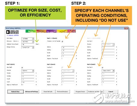
Figure 15. ADIsimPower software interface
The software intelligently selects the device and generates a complete bill of materials. The evaluation board can be applied directly within the tool. The design tool supports complex control of each channel, as shown in Figure 16.
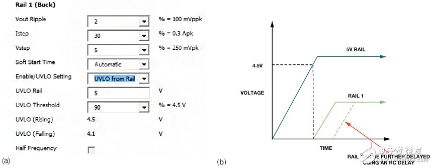
Figure 16. (a) You can specify the ripple, transient, and response for each rail.
(b) Use advanced timing control requirements that are precision enabled.
With ADIsimPower, power designers can quickly get accurate, tested reliability data, as shown in Figure 17.
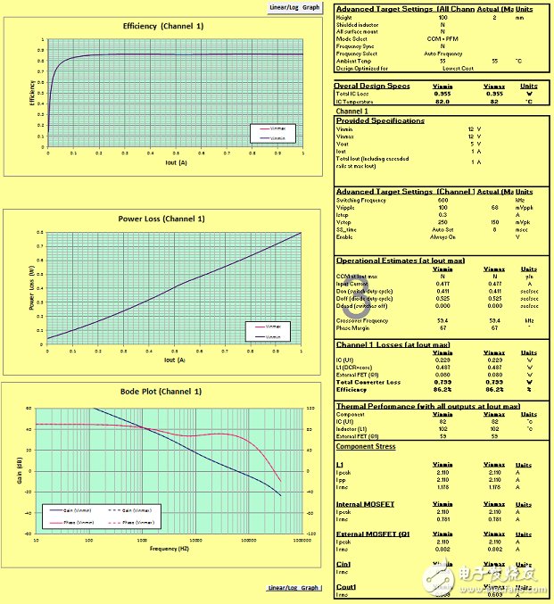
Figure 17. ADIsimPower simulation output
The design can then be assembled on the evaluation board as shown in Figure 18.
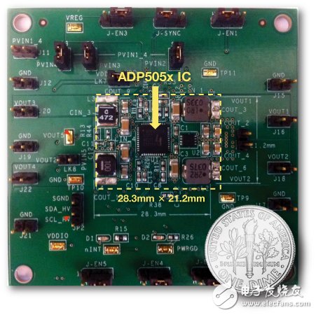
Figure 18. Power Circuit Using ADP5050/ADP5052
ADP5050/ADP5052/ADP5051/ADP5053 Technical Specifications
Product Model Description VIN (V)VOUT (V) Output Number Output Current (mA) I2C Main Characteristics Package Quote (USD/Piece)
ADP5050 Quad Buck Regulator, LDO, I2C Buck: 4.5 to 150.8 to 0.85 &TImes; VIN2 &TImes; Buck 4000, 2500 or 1200 is an I2C interface 48-pin LFCSP4 with independent enable pin and power good indication. 39
2 &TImes; Buck 1200
LDO: 1.7 to 5.50.5 to 4.75 LDO200
ADP5051 Quad Buck Regulator, POR/WDI, I2C Buck: 4.5 to 150.8 to 0.85 &TImes; VIN2 × Buck 4000, 2500 or 1200 is an I2C interface 48-pin LFCSP4 with independent enable pin and power good indication .59
2 × Buck 1200
ADP5052 Quad Regulator, LDO Buck: 4.5 to 150.8 to 0.85 × VIN2 × Buck 4000, 2500 or 1200 No Independent Enable Pin and Power Good Indicator 48-Lead LFCSP3.59
2 × Buck 1200
LDO: 1.7 to 5.50.5 to 4.75 LDO200
ADP5053 Quad Buck Regulator, POR/WDI Buck: 4.5 to 150.8 to 0.85 × VIN2 × Buck 4000, 2500 or 1200 No Independent Enable Pin and Power Good Indicator 48-Lead LFCSP3.79
2 × Buck 1200
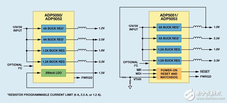
Figure 19. ADP5050/ADP5051/ADP5052/ADP5053: Quad Step-Down Switching Regulator with LDO or POR/WDI in LFCSP Package
in conclusion
The highly integrated new PMU enables complex power management solutions with high power efficiency, high reliability and ultra-small size. The combination of new design tools and flexible integrated circuits can reduce time-to-market for these complex power supplies. The ADP505x family is the latest in a portfolio of ADI's highly integrated, multi-output regulators that enable a single IC to be quickly and easily used in many different applications, reducing power supply design time.
Solar power is the ultimate renewable energy source whether you're an eco-minded consumer or practical individualist. The sun's light is sustainable energy that provides a resource that is renewable and has a very low carbon footprint. Solarhome is a premier provider of reliable, durable, proven photovoltaic systems from leading manufacturers, allowing you to harness this free energy alternative. Our grid-tie and battery backup options mean those cloudy days and long nights won't leave you without electricity.
250 Watt Solar Panel,Solar Panel,200 Watt Solar Panel,Solar Module
Yangzhou Beyond Solar Energy Co.,Ltd. , https://www.ckbsolar.com