Solar (PV) inverters convert the DC voltage generated by solar panels into AC voltage for use in public grids and commercial appliances. The optocoupler is an important part of this process because it prevents high voltages and transient voltages due to component damage or transmission distortion during the conversion process. This article will explore design techniques to improve the optocoupler power buffer to make it less susceptible to noise interference.
Optocoupler arm force solar inverter reliability increased
Solar panels typically produce high voltage DC output during the conversion of sunlight into energy. Converting the DC output to a high-voltage AC output minimizes line losses and allows the output power to be transmitted over long distances, either to the utility grid or to the building's internal grid where solar panels are installed. DC-to-AC (DC-AC) conversion is performed by a subsystem called a solar inverter, which can be designed as a single solar panel or as a central unit for converting solar panel arrays.
If the solar inverter is installed in a single solar panel, this is called a micro-inverter (Figure 1), which is a smaller solution for residential and general buildings where the power of the solar panels can be used directly in the building. The internal network of the object and commercial appliances. In this case, the inverter usually has a working power of less than 300 watts (W).
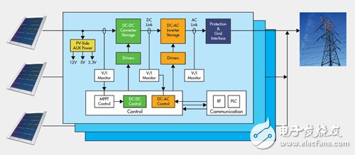
Figure 1 Micro-inverter architecture mounted on a single PV panel
When the solar inverter is used as a separate unit supporting several PV panels, it is called the Central Inverter (Figure 2). The block diagram is essentially the same as the micro inverter, but only one battery system. The energy of multiple solar panels can be stored and then delivered to the utility grid. The operating voltage of the central inverter is generally 1 kilowatt (kW) or more.
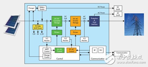
Figure 2 Central inverter architecture supporting PV panel array
When the optocoupler is integrated into a module that drives DC-DC and DC-AC converters, as shown in Figures 1 and 2. In both types of solar inverters, optocouplers are an important part of the system, preventing high voltage and transient voltages at one end of the line from causing component damage or transmission distortion at the other end.
When used to isolate high noise, high voltage, and high current circuits and low voltage control circuits, optocouplers can improve performance, make printed circuit board (PCB) smaller, and make circuit design easier. Isolating high-voltage components from low-voltage control circuits also helps protect grid workers or maintenance personnel who install, operate, or repair solar inverters.
Gate-driven optocoupler for solar inverters that drives high-speed MOSFETs and insulated gate bipolar transistors (IGBTs) and optimizes startup performance and noise immunity .
A gate-driven optocoupler capable of driving 1,200 volts (V) / 20 amps (A) IGBTs and MOSFETs with high levels of common mode rejection (CMR) for greater noise immunity; 100 nanoseconds (ns) Pulse Width Distortion (PWD) improves power efficiency, allowing designers to use smaller filters to reduce design size and cost; the PWD stage supports 1,414V operating voltage peaks to meet 1,200V IGBT switching.
Brief description of optocoupler operation
It can be used as an optocoupler for controlling the Power Buffer of a power MOSFET or IGBT gate. It provides a peak charging current for the gate of a power semiconductor in the form of a positive voltage (VOH), thereby turning on the device. The optocoupler pulls the gate of the drive device to zero voltage (VOL) or lower to turn off the gate.
MOSFETs or IGBTs are typically arranged in a half-bridge topology configuration. The drain of each high side N-channel MOSFET/IGBT is connected to the positive electrode terminal of the power supply, and each source is connected to the low side transistor. The source of the low side transistor is connected to the negative electrode of the system power supply.
Figure 3 is an internal block diagram of the optical coupler. Each part of the drive is powered by a common power supply or a bias supply. During startup, the complexity of the circuit causes a delay when the power is first turned on, which causes the gate output to increase with the VDD supply; it will continue to rise until the power supply is stable. Then, once the bias voltage is correct, the gate driver output returns to the correct state controlled by the light-emitting diode (LED).
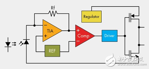
Figure 3 optical coupler block diagram
Set the order in which the power is turned on to minimize the effects of waiting for the optocoupler bias supply to stabilize. Solar inverters typically have one power supply, one logic supply (3.3, 5 or 10V), an optocoupler supply, and a high voltage supply to power the MOSFET/IGBT. Turn on in order of power supply, first logic power, then optocoupler power, and finally MOSFET/IGBT power. As a result, it helps to offset the effects of a stable bias supply. This turn-on sequence also satisfies the logic-controlled Power-on Reset and the Boostrap charging time of the isolated driver power supply.
For LED drivers, the forward current peak IF is "1A (1 microsecond (μs), 300 pps). The recommended operating current is 10?16 milliamperes (mA). Current rise time is less than 250 nanoseconds (ns), which minimizes transmission delay and reduces output switching jitter.
High-gain (23dB), high-power output optical amplifiers require a low-impedance supply over DC range up to 40MHz; use low ESR bypass capacitors and signal ground planes to help reduce spontaneous power supply noise and prevent output rise And the elimination of falling time.
Common mode rejection is a measure of noise
High-frequency transients are a type of noise that can damage the data transmission of the optocoupler's isolation barrier. The CMR is a measure of the ability of an optocoupler to withstand transient noise. CMR is one of the most important indicators to measure the performance of optocouplers. Other indicators include isolation level and working voltage.
The eight-pin DIP Coplanar optocoupler provides output capacitor high dielectric (Dielectric) insulation and low input. The eight-pin DIP package allows for creeping and gap distances greater than 8 mm (mm) and 0.5 mm insulation distance for reliable high voltage insulation.
Therefore, the gate driver optocoupler solution provides more insulation safety buffers, while the capacitive or inductive solution has an insulation distance of less than 0.1 mm. This improves safety and reduces noise coupling. This device uses coplanar optical coupling technology to block interference caused by electronic noise generated by load switching. There is also a special electro-optical mask that reduces the chance of capacitive coupling between switching transients and the active circuitry of the optocoupler.
A typical 240V AC power converter produces an 800V switching transient and a rotation rate greater than 6kV/μs. This large transient causes a 3mA peak current to flow between the input and output (for CIOs with only 0.5 picofarads (pF) of isolation devices). Figure 4 shows an example where a capacitor couples the noise current between the input and output of the coupler.
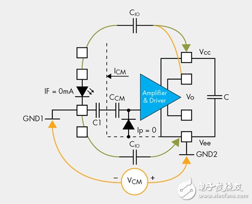
Figure 4 Current Mode Suppression LED "OFF"
Common mode transients have a negative voltage swing, the same as the coupler's output ground (GND2) reference; this transient pulls the output of the coupler to the output; the Package Capacitance is the CIO that provides the input and output. The main coupling impedance; when the LED is off, the output of the gate is low; if there is ample common mode current iCM drawn from the input to the optical amplifier, the amplifier will turn on.
The noise current iCM is extremely small because there is a special common mode mask that blocks the effects of electronic mask variations that minimize the coupling into or out of the optical amplifier, limiting the effective common-mode coupling capacitance to less than 50pF . In this way, the optocoupler can easily suppress positive or negative common mode transients with a maximum amplitude of 1.5kV and a rotation rate of more than 15kV/μs.
When the control current of the IF is equal to 10 mA through the LED, the driver output current is high and the source current flows to the load. Positive dv/dt will draw current from the amplifier to enhance the photocurrent; negative dv/dt will direct current to the amplifier, offsetting the photocurrent and possibly causing the amplifier to transition from high to low.
When IF is equal to 0 mA, the driver input is low and current is drawn from the load. A positive dv/dt pulls current from the amplifier and can cause the amplifier to transition from low to high. Negative dv/dt introduces current into the amplifier and helps maintain the amplifier to maintain the output low.
In general, minimizing the coupling capacitance between logic control and power semiconductors can greatly reduce the ability of common mode noise transients to become normal mode pulse noise. Using a low and balanced impedance at the drive point improves interference immunity and power MOSFET control using Galvanic Isolated drivers minimizes common-mode noise coupling.
Split LED boosts half-bridge configuration performance
Common-mode transient suppression is especially important in half-bridge topology configurations because switching transients during normal current operation may cause the closed gate drive to turn on. The shunt LED can be used to increase the current-resistance transient capability of the half-bridge configuration and maintain the load dv/dt coupling of the package capacitor at low impedance - for running LEDs or running BJT Or the on-state resistance of the logic gate. However, the disadvantage of this approach is that increasing the shunt LED drive will reduce efficiency because the circuit consumes power regardless of whether the LED is turned on or off. Figure 5 shows a sample configuration.
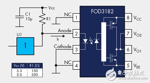
Figure 5 Optocoupler architecture with shunt LED driver
The LED is connected in parallel with the drive switch to form a current shunt drive. U1 is an open drain logic gate that acts as a driver. When the switch is off and U1 is high, LED current will pass. To turn off the LED, the gate must be forced low, which reduces the voltage across the LED to less than the desired forward voltage value. It also provides low impedance and reduces the effects of common mode conduction current on LED operation.
Understand the maximum switching frequency of the optocoupler
When using an optocoupler, it is useful to know the maximum switching frequency of the design. This calculation involves two basic steps. First, it must be determined that the optocoupler output driver MOSFET can diffuse at a maximum operating junction temperature of 125 ° C and a room temperature of 100 ° C. Maximum power. Second, determine the diffuse RMS power of the output transistor and the RDS(ON) voltage drop across the optocoupler transistor for the charge and discharge currents of a given MOSFET gate.
Solar inverters play an important role in generating and transmitting clean and sustainable energy. When performing DC-AC conversion, the high-voltage current must be carefully and effectively isolated, and the optocoupler is suitable for this power buffer. If you pay special attention to the startup requirements and use related technologies to improve the anti-interference ability, you can help optimize the performance of the optocoupler.
The gate-driven optocouplers described in this article are compatible with discrete power MOSFETs and IGBTs, so designers can unify the logic, isolation, and MOSFET sections of the power conversion circuitry. The solution converts milliwatts (mW) to kW while providing isolation between the primary and secondary circuits.
LED Flood Light made by aluminum alloy. Surface coating by special technology or anodizing aluminum process, impact resistant,sturdy and durable features. Fins design of heat,rational utilization cross-ventilation to improve products stability and working life.
SMD LED Flood Light, the Waterproof level of LED Flood Light is IP65.IP66.IP67.All of them applied in commercial and residential.
LED Flood Light
LED Flood Light,High Power LED Floodlight,LED Outdoor Flood Lighting,Explosion Proof LED Flood Light
Wenzhou Korlen Electric Appliances Co., Ltd. , https://www.korlenelectric.com