The main reason why power GaN lags behind RF GaN is that it takes time to implement the cost reduction strategy used by several vendors. The best known is the switch to a 6-inch silicon substrate and a lower cost plastic package. For power supply designers, it is important to understand the performance improvements that GaN is likely to bring, as well as some degradation mechanisms that can affect the performance of the final product over time.
The Joint Electronic Equipment Engineering Council (JEDEC) certification standard for silicon devices has proven to be a good predictor of product lifetime, but there is currently no equivalent standard for GaN. To use new technologies to mitigate risks, it is prudent to take a look at specific use cases, as well as the environmental limitations of new technologies in application, and to build prototypes that can stress test and monitor for environmental changes. Real-time monitoring of a large number of prototypes presents some interesting challenges, especially when the GaN device voltage is close to 1000V and dv/dts is greater than 200V/ns.
A chart that is often used to determine if a power FET can meet the target application requirements is a Safe Operating Area (SOA) curve. An example is shown in Figure 1.
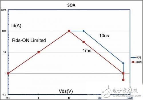
Figure 1: Example of a GaN FET SOA curve, where Rds-On = milliohms
Hard switch design
Power GaN FETs are used in hard switching and resonant designs of several MHz. The zero voltage (ZVS) or zero current (ZCS) topology shown above is several kilowatts. The region where the stress of the SOA curve is the largest is the region where the voltage and current in the upper right corner are the highest. Running a power GaN FET in this hard switching region results in an increase in stress caused by several mechanisms. The easiest to understand is thermal stress. For example, when using an inductive switch test circuit, it is possible to make the device almost zero when the device is turned off, draw a voltage of several hundred volts, and switch the current to almost instantaneously to 10A.
The voltage on the device is multiplied by the current flowing through to obtain instantaneous power dissipation. For this example, it can reach more than 500W in the middle of the conversion. For a typical power GaN device measuring 5mm x 2mm, this value can reach 50W per mm2. So the user does not need to be surprised that this area of ​​the SOA curve only supports short pulses. Due to the thermal limits of the device and the package, the upper right portion of the SOA curve is considered to be a function of pulse width. Due to the thermal time constant seen in the curve, shorter pulses result in less heat dissipation. Enhanced packaging technology can be used to reduce junction-to-ambient thermal resistance from approximately 15 °C/W to 1.2 °C/W. This approach can expand SOA by reducing device heat dissipation.
SOA curve
TI has a range of standard footprint power MOSFETs, DualCool? And NexFETs? . These MOSFETs dissipate heat from the top and bottom of the package and provide 50% higher current than traditional footprint packages. This gives designers the flexibility to use higher currents without the need to increase the size of the terminal. One of the great advantages of GaN FETs compared to silicon FETs is the extremely short switching times that can be achieved. In addition, the reduced capacitance value and the negligible Qrr make the switching losses much lower. When the device is switched, the integer part of the value obtained by multiplying the voltage by the current is the power that the device must consume. Lower losses mean lower device temperatures and greater SOA.
Another important area circled by the SOA curve is limited by Rds-On. In this region, the voltage across the device is the current flowing through the device multiplied by the on-resistance. In the example of the SOA curve shown in Fig. 1, Rds-On is 100 milliohms. The temperature of silicon MOSFETs depends on their Rds-On, which is well known. When the device temperature rises from 25oC to about 100oC, their Rds-On is almost doubled.
Dynamic Rds-On
GaN FETs have a complex Rds-On that is a function of temperature, as well as voltage and time. The dependence of Rds-On on GaN FET on voltage and time is called dynamic Rds-On. In order to predict how a GaN device will operate for a target, it is necessary to monitor the impact of these dynamic Rds-Ons. Similar to the temperature-introduced stress of the SOA curve, the inductive hard-switching stress circuit is more suitable for monitoring Rds-On. This is because many potential device degradations are associated with high frequency switching and electric fields.
Figure 2 is a simple switching circuit in which a method of implementing a circulating current in the upper right quadrant of the SOA and applying stress to the device is presented.
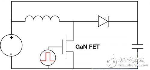
Figure 2: Inductor hard switch test circuit
Wide band gap
GaN is a wide bandgap material with a bandgap of 3.4 eV compared to the 1.12 eV bandgap of silicon. This wide bandgap allows the device to support much higher electric fields than silicon devices of the same size before being broken down. Tests commonly used by some device designers to help determine device reliability include high temperature reverse bias (HTRB), high temperature gate bias (HTGB), and time-dependent dielectric breakdown (TDDB). These are static tests, although they are a good way to verify the effectiveness of device design, but when high frequency switching dynamics dominate, it is not representative of typical use. High Temperature Operating Life (HTOL) is a dynamic test during device switching. The specific operating conditions are determined by the manufacturer, but these operating conditions are typically at some nominal frequency, voltage, and current.
Early studies on the use of GaN for RF amplifiers found a performance degradation effect, at which point the maximum current that the device can deliver is reduced as a function of the drain voltage bias. This voltage-dependent (capture introduction) effect is called "current collapse." The negative charge trapped at the buffer and top layer causes current collapse or dynamic Rds-On increase. When a high voltage is applied, the charge can be trapped and may not dissipate immediately when the device is turned on. Several device design techniques (electric field plates) have been employed to reduce the electric field strength in most sensitive GaN FET regions. The electric field plate has been shown to minimize this effect in RF GaN FETs and switching power GaN FETs.
GaN is a piezoelectric material. GaN device designers take advantage of this piezoelectric effect by adding an AIGaN buffer layer with a slightly mismatched lattice. Doing so increases the stress on the device, resulting in a polarization field caused by spontaneous and piezoelectric effects. This two-dimensional electron gas (2DEG) channel is the product of this polarization field. Devices with 2DEG channels are known as High Electron Transfer Transistors (HEMTs). Unfortunately, high applied electric fields can also cause harmful piezoelectric stresses while the device is operating, leading to another form of possible device degradation. For new technologies such as GaN, it is important to have a comprehensive approach to proven reliability. For further details related to the TI program, please refer to Sandeep Bahl's white paper, a comprehensive approach to defining GaN products.
In order to reduce costs, power GaN is currently using a 6-inch silicon substrate. Thread dislocation occurs due to a mismatch between the silicon and GaN lattices. This can lead to lattice defects and increase the likelihood of capture. The impact of these captures depends on their number and location in the device. The capture state, occupied or unoccupied, is also a function of the applied electric field and time. Capture charge and discharge may be distributed over a time range from a minimum of 100 ns to a maximum number of minutes. The capture charge and discharge closest to the gate region modulate the transduction of the device. All of these effects are the basis for the complex voltage and time correlation of the GaN FET's Rds-On. During the definition period, the engineer typically applies DC stress to the device for an extended period of time and periodically removes this stress to describe the condition of a single semiconductor test. By removing the device voltage offset, some capture discharges can be achieved even in a matter of seconds, so that the dynamic Rds-On values ​​associated with the actual operation are not affected.
to sum up
Power GaN FETs have many advantages over silicon FETs, such as lower switching losses and higher frequency switching capabilities. Higher switching frequencies can be used to increase the power conversion density of the system. To define a system that is using power GaN FETs, designers should be aware of possible sources of degradation and monitor their effects over temperature changes. An easy way to monitor the dynamic Rds-ON increase is to measure the efficiency of the conversion process during time and voltage changes. To better understand where losses occur, the system is designed to monitor the drain, gate, source, and device current waveforms in real time. This system is capable of hard switching FETs through their SOA at frequencies above 1 MHz, at voltages up to 1000V and currents up to 15A.
Capturing and analyzing real-time waveforms can help us better understand high-frequency effects such as dv/dt, gate driver inductance, and board layout, all of which are critical in GaN-based designs. Monitoring real-time information on trends in time and temperature ranges provides us with better GaN FET degradation information and gives us an in-depth understanding of the needs of smarter devices and controller products.
CE approved input 220V output AC24V CCTV power distribution unit led transformer power supply box
Features:
- Thermal Cutoffs Protection (TCO): each output has independent PTC fuse and LED indicator, when problem occurs, only affect the independent output, other outputs still working.
- Short circuit protection: when short condition occurs, independent PTC fuse will open the circuit, when condition removed, PTC fuse will automatically back to close.
- High voltage protection: when high voltage occurs, the surge protection will be hit through to protect the connected device.
- Over Current protection: when over current occurs, the power supply will automatically switch to self-protection status, when condition removed, then switch back to normal.
- Integral Surge Protection:
Soft starting current, effectively reduce the impact of AC input, independent short-circuit protection and surge protection, resume automatically after clearing of fault, EMI filter, minimum ripple, 100% load test, quality guarantee, high efficiency, low T-rise, continuous duty.
Individual LED Power Indication:
Input with a switch, LED indicators lighten when the power supply operates normally.
Individual PTC Output Protection:
each output contains independent PTC, LED indicator, which is not interfere with each other.
Application:
- Security Monitoring system
- Multimedia Network Teaching System
- Medical Monitoring Display System
- Industrial Automation Control System
- Banking ,securities,financial information display system
- Remote Network Server Monitoring
- Department Store Security
Product Images:

Boxed Power Supply,Boxed Power Supply 24Vac,Cctv Boxed Power Supply, Boxed Power Supply Ups
Guangdong Steady Technology Co.LTD , https://www.steadysmps.com