This article describes a circuit that clamps the input voltage to the maximum voltage required while still maintaining high current transfer capability and minimizing losses during periods of no transient voltage.
This article refers to the address: http://
Circuits powered by automotive electrical systems must operate in harsh environments. Transient voltages include random transient voltages and periodic transient voltages. Periodic transient voltages—such as starting the engine—can produce hundreds of volts, but the most serious transients for automotive electronics come from load-dump.
When the alternator supplies a charging current to the load, the sudden release of energy caused by the rapid disconnection of the battery is the load dump. In addition, due to the use of batteries stacked in series, an overvoltage condition can be generated when the car is started. Other transient phenomena are ignition system noise, relay opening and closing, and one-time events such as blown fuses.
Fortunately, most of the violent high-energy transient voltages or currents can be handled by interference suppressors; typically, they are located near critical (and expensive) components that have high-impedance paths to the source. The vehicle's interference suppressor must be able to withstand repeated load dumps with peak power consumption exceeding 1,500W and limit battery rail drift to less than ±40V.
Additional protection circuitry usually requires further adjustment of the voltage rail. The reverse polarity diode is connected in series with an additional load circuit on the battery rail to effectively suppress negative voltage spikes. Whether the design engineer can clamp the transient voltage below +40V depends on the circuit receiving the voltage. The DC-DC regulator that receives the power from this voltage must be able to withstand at least +40V to prevent overvoltages in the power components and control circuitry. Most modern pulse width modulation (PWM) controllers cannot withstand voltages greater than +40V without sacrificing useful functions, such as the synchronization required to meet design specifications.
For light load currents typically less than 0.1A, the only effective way is to use current limiting resistors and clamp Zener diodes to keep the series resistance loss not too large. The circuit depicted below provides a way to clamp the input voltage to the maximum voltage required while still maintaining high current transfer capability and minimizing losses during "typical" non-transient operation.
In the design of the circuit, the output voltage is limited to 27V by Zener diode D2. The output voltage is intended to be powered by a DC/DC converter with an absolute maximum voltage rating of 30V. For a steady-state input of 12V, transistor Q2 is in the "off" state, and resistor R3 pulls the gate of p-channel FET Q1 to ground, thereby turning Q1 on.
For input voltages greater than approximately 3V, Q1 begins to conduct current; and is fully enhanced at 4.5V. The voltage drop across Q1 is quite low and is determined by its Rds-on rating and output load current. For example, when the input is 14V and the load current is 3A, the voltage drop across Q1 is only 0.16V. For high input voltages, diode D1 prevents FET Q1 from exceeding the maximum 20V gate-to-source threshold voltage. For designs where the input voltage does not exceed 20V, D1 is not required.
As the input voltage rises, the output will follow the change in the input voltage until the breakdown voltage of Zener diode D2 is reached and current is conducted. At this point, the output voltage is clamped to the sum of the terminal voltages of the three components Zener diodes D2, R4, and R6. The sum of the voltages across R4 and R6 is only about 0.6V.
Transistor Q3 is configured as an emitter follower and thus has a current gain of approximately one. Since the collector current flows through Q3, it biases Q2 to begin reducing the gate-to-source voltage of FET Q1. The output voltage is held at 27.6V because FET Q1 reduces the extra input-output voltage across it, acting as a linear regulator. As the input voltage increases, the output does not increase because additional current flows through Zener diode D2 and forces Q2 to lower the Q1 gate source drive voltage. This closed loop feedback prevents changes in the output voltage.
The voltage clamping circuit limits the output voltage to 27V
System stability
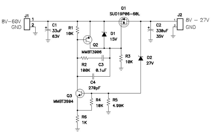
Due to the use of a negative feedback closed-loop control system, stability is critical to predictable and reliable operation. The closed-loop gain and phase margin determine how well the system responds to external disturbances, such as changes in input voltage.
Transistor Q3 is intentionally configured as a unity gain in order to introduce no additional gain into the feedback path. Transistor Q2 provides a current gain equal to its beta, typically between 50 and 200. FET Q1 also provides a gain equal to the output load resistance multiplied by the transconductance, which is also on the order of 200. The total closed-loop DC gain is the product of these two gain terms, which is quite large, greater than 80 dB. The load resistor and output capacitor introduce a pole in the transfer function to roll the gain of FET Q1 down to -1 slope or -20dB/decade over 50Hz. The equivalent series resistance (ESR) of the output capacitor also adds a zero point set by the ESR and its capacitance. This flattens the frequency response above 6KHz. Careful formation of the frequency response of the Q2 gain provides an overall acceptable closed-loop frequency response.
The compensation network consisting of R2, C3 and C4 makes the necessary trimming of the frequency response curve. The gain of Q2 decreases from a direct current with a slope of -1 until the zero introduced by the series combination of R2 and C3. This zero is aligned to the pole near 50 Hz. The parallel combination of R2 and C4 introduces a pole aligned with the 6KHz zero. The total effective loop gain now maintains a -1 slope drop until the unity gain is exceeded, as shown in the following figure. The example circuit shows that under almost all load conditions, the load current is greater than 0.5A and the phase margin is 90 degrees with a bandwidth of at least 70KHz. Because there are low frequency poles set by the load resistor and output capacitor, the bandwidth decreases as the load resistance increases.
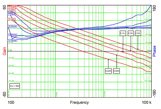
The figure below shows the response of the output voltage to a large, irregular transient input voltage. Once the input voltage exceeds the nominal value of 27V Zener diode D2, the output voltage is clamped and plays a good role in suppressing further changes in the input.
The output voltage is clamped to the desired level (red)
In order to prevent the FET Q1 from being overvoltaged, several important factors must be considered. The voltage, current, and power pressures on Q1 must be maintained within the safe operating area (SOA) curve of the device. Heavy loads and large voltage drops across Q1 (with constant overvoltage conditions) will push the device to the limit. If working outside the SOA curve, the FET will dissipate a very large amount of power, and since the device may not have thermal conduction capability, it cannot dissipate heat in such a short period of time, and eventually the FET may fail.
In addition, if the slope of the input transient voltage changes very high and the resistance in series with the input source voltage is small or absent, it will result in extremely high peak input current, which may again exceed the safety specified by the SO1 curve of Q1. The scope of work. For this reason, it is necessary to connect a large enough resistor in series with the input to limit the peak input surge current flowing through Q1. A slowly varying input voltage will also help limit the peak input current.
Summary of this article
The input clamp circuit described herein provides a low cost method of clamping the output voltage to a safe level, preventing potential damage to the low voltage circuit from overvoltage. The circuit can be easily clipped by setting the output clamp voltage and load capacitance and adjusting the control loop. Under typical input conditions, the forward voltage drop of the pass element is relatively low, resulting in low losses, which is higher than that achievable with a linear regulator.
This battery is for replacing Lead-Acid Battery, it has the standard appearance and size as well as capacity, but longer cycle life and high energy and good charge and discharge performance.
Capacity:100AH/150AH/180AH/200AH/250AH.
Voltage:12.8V, cycle life is more than 2000 times, also can customize the capacity.
Rechargeable Lithium Battery,Lithium Polymer Battery,Rechargeable Lithium Ion Batteries,Rechargeable Lithium-Ion Batteries,12v 200Ah Powerful Bank,Home Storage Rechargeable Battery
Shenzhen Enershare Technology Co.,Ltd , https://www.enersharepower.com