1 Introduction
This article refers to the address: http://
The use of thin film technology to fabricate thin film circuits is an important branch in the field of thin films. Main features of the thin film circuit: high manufacturing precision (low film line width and line spacing), small hole metallization, integrated passive components such as resistors, capacitors, inductors, air bridges, etc. A multilayer circuit is fabricated using a medium. The thin film multilayer circuit refers to a thin film process such as vacuum evaporation, sputtering, electroplating, and a pattern forming technique such as wet etching and dry etching (reactive ion etching, plasma etching, laser etching) on ​​a polished substrate. A multilayer interconnection structure in which a conductor (Cu or Au, etc.) wiring and an insulating dielectric film (PI or BCB or the like) overlap each other is formed on a material (ceramic, silicon, glass, or the like).
Thin-film multilayer circuit technology is very competitive in the microwave field due to its high interconnect density, high integration, high-power circuit manufacturing, and system-level functions of the entire package structure, especially on the airborne. In the spaceborne or aerospace field, its small size, light weight and high reliability are more prominent. It is a very promising microwave circuit module (low noise amplifier, filter, phase shifter, etc.), and even more demand The larger the T/R component substrate manufacturing technology.
Based on the analysis of the characteristics of the application of thin film circuits in T/R components, this paper introduces several typical application examples and gives development suggestions.
2. Analysis of the characteristics of thin film circuit technology applied in T/R components
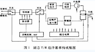
With the development of radar technology, active phased array radar has become the mainstream, and its core is the T/R component, which usually contains thousands of T/R components per radar. T/R components are basically the same regardless of whether they are used at the same frequency or whether they are used in the same place. They are mainly composed of power amplifiers, driver amplifiers, T/R switches, phase shifters, limiters, and low noise. Amplifier, looper, logic control circuit, etc., its structural block diagram is shown in Figure 1 (1). These basic components, when the process is implemented, can be directly used on the circuit board, such as microstrip transmission lines, switches, couplers, filters, etc., some use external chip (such as power amplifier, drive, etc.), capacitors, loopers Wait to achieve. Therefore, from the use function and structure, the T/R component can actually be regarded as a microwave multi-chip module with transceiving function.
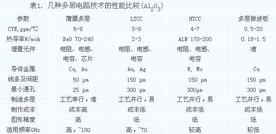
Due to the radar beam grating effect (the center distance of two adjacent radiating elements is less than half of the working wavelength) and the limitations of weight and cost, the miniaturization, integration and weight reduction of T/R components will be its development trend. In order to meet its performance requirements, it is inevitable to develop and produce T/R components by using multi-layer integration technologies such as low temperature co-fired ceramic LTCC, high temperature co-fired ceramic HTCC, thin film multilayer circuit technology and multilayer microwave printed circuit technology. A comparison of the multilayer techniques is shown in Table 1 (2~3).
As can be seen from the table, the thin film multilayer interconnection substrate has the following outstanding advantages:
(1) The wiring density is high, the volume can be small, and the weight is very light;
(2) High integration, it can embed passive components such as resistors, inductors, capacitors and active chips;
(3) Good high frequency characteristics, can be used in the field of microwave and millimeter wave;
(4) With high power density, high-density high-power multilayer substrates can be fabricated by using high-heat-conductivity metal, diamond, ceramic or aluminum carbonized silicon composite materials.
Thin film multilayer interconnect substrates have the following significant disadvantages compared to other types of substrates:
(1) The process adopts a string type, the yield is relatively low, and the manufacturing cost is high;
(2) The number of manufacturing layers is limited.
Thin film multilayer circuit technology has obvious advantages and disadvantages, so there are two options for the choice of manufacturing T/R components. First, the T/R module (4~5) can be directly fabricated on a ceramic substrate or a metal substrate by using a thin film technology, and the film has high precision, high integration, and high power performance, and the method is costly; Combining thin film technology with other multilayer circuit technologies (such as thick film technology, HTCC, LTCC, etc.) (6-8), manufacturing T/R components, making advantages and avoiding shortcomings, not only making the other substrates easy to realize multi-layer characteristics, thus overcoming the film The shortcomings of the technology itself are insufficient to produce layers, and the high precision and high performance of the thin film technology itself can be exerted.
3. Application examples of thin film technology in T/R components
3.1 Thin film hybrid integrated T/R assembly on ceramic substrate
RCA Lab reported in 1985 that the T/R module (3) was fabricated on a high thermal conductivity ceramic BeO substrate using a thin film process. The dimensions were 7.0 cm x 9.0 cm x 1.6 cm, the operating frequency was 16.0 to 16.5 GHz, and the peak power was 3.9~. 4.4 W, voltage tuning range 2.5~2.9, noise figure 5dB.
Martin Marietta Labs first reported in 1995 the use of thin-film technology to manufacture a W-band 8-cell T/R assembly with a frequency of up to 94 GHz (4), as shown in Figure 3. The dimensions of the assembly are 16.5 mm x 28.3 cm x 1.8 cm with a maximum gain of 47.8 dB. The main process is to first manufacture DC and control signal boards on a 0.5 mm thick molybdenum substrate using a copper conductor and polyimide film multilayer process, and then fabricate it on a 0.125 mm thick low loss Al2O3 ceramic plate. RF transmission line, and finally the RF part and chip, capacitor, etc. are assembled on the low frequency motherboard.
3.2 Thin film hybrid integrated T/R components on metal substrates
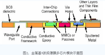
The production of T/R modules or multi-chip modules on metal substrates such as aluminum and molybdenum has also been reported in recent years (4-6). In 1995, Australia's O.Sevimli reported on a metal-based V-band (up to 110 GHz or more) thin-film multi-layer multi-chip module patent technology (5), the structure is shown in Figure 2. The technical process is as follows: firstly, the hole for mounting the chip is etched on the metal substrate, and then the chip is fixed in the hole by using a conductive adhesive, and the depth of the hole for mounting the chip is controlled so that the chip is in the same metal surface In-plane and precise positioning, the surface is coated with a dielectric material such as BCB suitable for use in the millimeter wave field, and finally the through hole is etched at the die pad to fabricate the thin film multilayer circuit. The outstanding advantage of this technology is that all chips or passive components (such as couplers, filters, etc.) can be assembled at the same time. The assembly does not use gold wire bonding or flip chip to solve the millimeter wave band gold wire bonding tape. The consistency control and parasitic problems come into being; at the same time, the power dissipation problem caused by flip chip can be solved, and the heat of the chip can be quickly dissipated through the metal base plate.
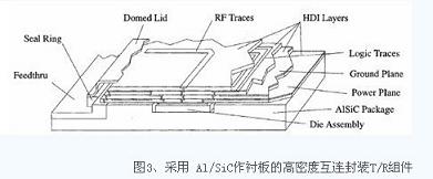
3.3 HDI technology T/R components on A l/SiC composite substrate
In 1997, Lockheed Martin reported the T/R component (7) of a thin-film multilayer circuit based on an Al/SiC substrate developed by GE. The structure is shown in Figure 3. The substrate using T/R component made of Al/SiC material mainly considers that the material has high thermal conductivity (close to aluminum nitride, about 160W/moK), and the thermal modulus is close to that of GaAs or Si active chip, which is beneficial to direct Mount the chip. In addition, the material has a low density, which is advantageous for reducing the weight of the component. Al/SiC material is used as the substrate, which must be pre-formed and Ni/Au plated. The active chip and passive components can be directly mounted in the cavity and placed on the same plane as the substrate surface. The power GaAs chip is soldered into the cavity of the substrate by AuSn high temperature solder to ensure heat conduction and reduce the junction temperature of the device; the non-power chip and the passive device can be adhered to the cavity of the substrate by using conductive paste. Then, the HDI technology (thin film high-density multilayer interconnection) is implemented thereon, that is, a layer of polyimide film (kapton) is laminated with an adhesive, and a laser is used to open holes in the corresponding chip pads and the required positions on the substrate. Metallization (Ti/Cu/Ti) is performed on the substrate by a sputtering process, and then the pattern and the strip line are formed by laser or photolithography. And so on, to achieve multiple layers.
3.4 Thin and thick film hybrid integrated circuit broadband T/R components
In 1992, GM reported a wideband S/C-band T/R component (8) (3.0 to 6.0 GHz) developed using a thin film and thick film hybrid process, measuring only 3.3 inches by 1.17 inches, and S-band output power of 21W, C. The band output power is 19W and the receiving gain is 30~38 dB. The structure diagram is shown in Figure 4. On the same alumina ceramic substrate (0.635mm thick), the front side uses thin film technology for microstrip circuit, the back side uses thick film technology for 4-layer wiring, front thin film circuit and back thick film circuit. The interconnection between the two is achieved by laser drilling, and the chip and device are buried in the hole of the ceramic plate.
3.5 Thin film multilayer emission module on semiconductor silicon material
On semiconductor silicon materials, the advantages of using thin-film multilayer technology to fabricate T/R components are that they can be compatible with semiconductor technology, and can integrate active chips and passive components. The components can be made small and can be mass-produced. Due to the low thermal conductivity of silicon materials, high thermal conductivity aluminum nitride and yttria ceramics are more advantageous when high power or high Q is required. Figure 5 is a schematic diagram of a thin film multilayer emitter module developed by the University of Cincinnati, USA. It is made of a polyimide of Dupont Company on a silicon substrate (the thickness of each layer is 9~15μm), using Ti-Au- Ti or Cr-Au-Cr is used as a conduction band (Au thickness 2~3μm), and a multilayer interconnection structure of 4 layers of metal and 3 layers of medium is fabricated.

3.6 Thin film multilayer T/R components on HTCC substrates
The T/R component (7) of the HTCC substrate-based thin film multilayer circuit developed by GE and Lockheed Martin, as shown in Figure 7. The HTCC substrate is pre-grooved and metallized, and the power chip is placed in the pre-groove to be level with the surface of the substrate, and then the HDI process is performed thereon.
The substrate using HTCC as the T/R component is to take full advantage of the advantages of high temperature co-fired ceramics (HTCC) and thin film multilayers, while avoiding its shortcomings. The advantage of HTCC is that it has high thermal conductivity and easy to realize multiple layers; its disadvantage is that the conductive loss is large due to the use of Mo, W and other pastes with high resistivity. The advantages of thin film multilayer interconnection technology: high line precision, using materials with low resistivity such as Cu and Au as conduction bands, and low microwave loss; the disadvantages are insufficient power resistance and high multi-layer cost. HTCC-based thin-film multilayer interconnect technology can distribute power lines, ground planes, and signal lines in HTCC to meet power-tolerant requirements and reduce the number of layers of thin films. The power chip can be soldered to the cavity of the HTCC to facilitate heat dissipation. Microstrip lines and chip fine interconnects can be used in a few layers of HDI layers to meet microwave performance requirements.
3.7 Thin film integrated T/R components on LTCC substrates
Reinhardt Microtech and Micro Systems Engineering have teamed up to develop a Finebrid integration technology for X-band T/R components that integrates LTCC and thin-film technology in DuPont 951 or 943 The LTCC board made of porcelain is directly processed into a thin film circuit pattern without polishing or the like. The structure is shown in Fig. 8. It is easy to realize the characteristics of multiple layers by using LTCC. The DC power supply line and the control signal line are made on different layers, and passive components such as resistors and capacitors can be buried. DuPont 951 or 943 raw porcelain was chosen because the LTCC loss was relatively small. Passive components (such as Lange couplers, filters, resistor networks, attenuators, power splitters, etc.) are integrated on the LTCC surface using the high precision of the film. In practical use, the film pattern has a typical line and pitch of 20 micrometers and a film thickness of 5 micrometers; the NiCr layer acts as a resistive layer and an adhesive layer. As can be seen from the structure diagram, the chip is mounted in the cavity of the surface of the LTCC, which can reduce the bonding length and the associated inductance. The heat of the chip can be transmitted to the lower heat sink through the heat dissipation through-hole column on the back surface, which can overcome the LTCC heat. The disadvantage of low conductivity. After reliability testing, the thin film process on the LTCC surface is comparable to the reliability on alumina ceramics.
4. Conclusion
It can be seen from the above analysis that compared with the traditional thin film process on ceramic substrates, the application of thin film technology in T/R components has two distinct new trends. First, in high thermal conductivity metals, alloys and composites. Multi-layer thin film process (Al/SiC) is used to manufacture T/R components, which improves the power resistance of the components and facilitates packaging. The chip can be placed in the cavity of the surface according to the design requirements, and the gold wire is shortened. Bond length or no bonding, reduce or overcome parasitic effects, improve component performance; second, on other multi-layer substrates (such as HTCC or LTCC), implement thin film process to manufacture T/R components, give full play to HTCC or LTCC is easy to realize the advantages of multi-layer and embedded passive devices and the high precision and low loss of thin film process. It is of great significance to reduce the size of T/R component substrate and improve the electrical and thermal properties of components.
Domestically, in the manufacturing field of T/R components, relevant application reports have not yet been seen, and attention can be paid to carry out related follow-up research work.
Reel with solid flanges, turned on the drum and in the central bore. The available sizes are as per DIN 46395 / 46397 specifications or as indicated by the Customer, for a normal use up to 1400 mm of flange diameter.
Indicated for metallic wires. To be used on a wiredrawing, stranding or rope-making machine. It withstands annealing treatment.
| Serial Number | Specification Model | Lateral Plate Diameter D1 | Major Diameter D2 | Axle Hole Diameter D4 | Carrying Hole Diameter D5 | Center Distance E of Axle Hole and Carrying Hole | External Width L1 | Internal Width L2 | Remarks |
| 1 | 285 | 285 |
130 165 |
127 | 18 | 180 | 260 | 240 | Thin Extend Shaft |
| 2 | 300 | 300 |
130 165 |
127 | 18 | 180 | 270 | 250 | Thin Extend Shaft |
| 3 | 335 | 335 |
165 217 |
127 | 18 | 180 | 270 | 250 | Thin Extend Shaft |
| 4 | 400 | 400 |
217 270 |
125 127 |
18 | 100 | 270 | 250 | Middle Extend Shaft |
| 5 | 500 | 500 |
217 270 |
125 127 |
22 | 130 | 320 | 300 | Middle Extend Shaft |
| 6 | 630 | 630 |
350 420 |
125 127 |
28 | 200 | 430 | 400 | Twist Extend Shaft |
| 7 | 300 | 300 |
130 165 |
56 | 8 | 100 | 290 | 270 | Twist Extend Shaft |
| 8 | 335 | 335 |
130 165 |
56 | 8 | 100 | 290 | 270 | Twist Extend Shaft |
| 9 | 400 | 400 |
165 217 |
70 | 16 | 170 | 270 | 250 | Extend Shaft |
| 10 | 500 | 500 |
217 270 |
80 | 16 | 100 | 320 | 300 | Extend Shaft |
| 11 | 560 | 560 |
270 295 |
80 | 18 | 120 | 355 | 329 | Extend Shaft |
| 12 | 610 | 610 |
270 320 |
80 | 22 | 170 | 360 | 336 | Extend Shaft |
| 13 | 630 | 630 |
355 450 |
125 127 |
28 | 200 | 360 | 336 | Extend Shaft |
| 14 | 710 | 710 |
400 500 |
125 127 |
28 | 100 | 530 | 450 | Extend Shaft |
| 15 | 800 | 800 |
450 560 |
125 127 |
28 | 100 | 600 | 500 | Extend Shaft |

Flat Wire Spool, Panel High-speed Spools, Empty Spool, Cable Spools
NINGBO BEILUN TIAOYUE MACHINE CO., LTD. , https://www.spool-manufacturer.com